STMicroelectronics STP22NM60
This improved version of MDmesh™ which is based on Multiple Drain process represents the new benchmark in high voltage MOSFETs. The resulting product exhibits even lower on-resistance, impressively high dv/dt and excellent avalanche characteristics.| Part No. | STP22NM60 |
|---|---|
| Datasheet | STP22NM60 Download |
| Manufacturer |  STMicroelectronics |
| Description | N-CHANNEL Power MOSFET |
| Buy | Stock & Price |
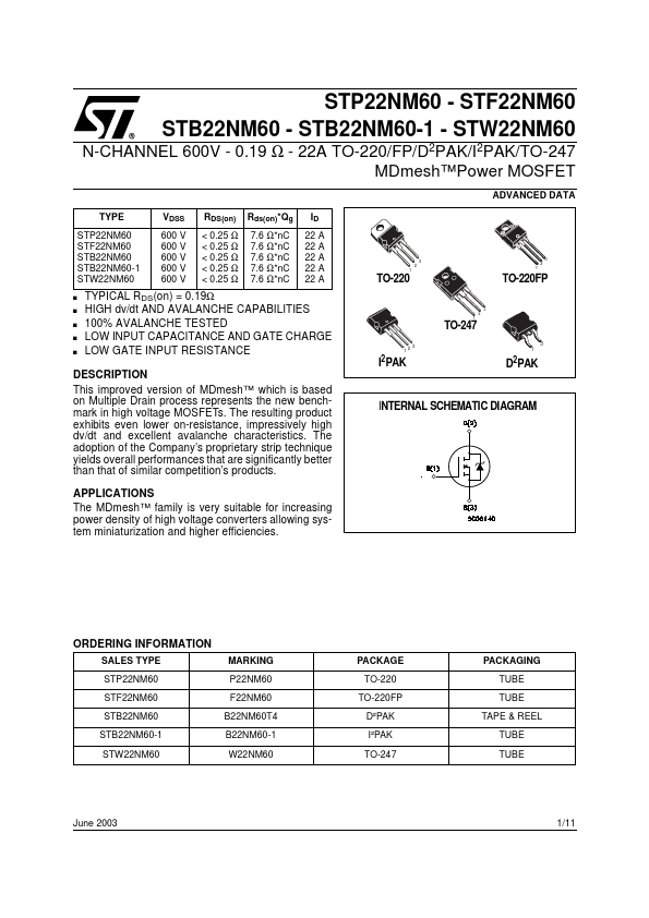
DESCRIPTION
The adoption of the Company’s proprietary strip technique yields overall performances that are significantly better than that of similar competition’s products.APPLICATIONS
The MDmesh™ family is very suitable for increasing power density of high voltage converters allowing system miniaturization and higher efficiencies. INTERNAL SCHEMATIC DIAGRAM ORDERING INFORMATION SALES TYPE STP22NM60 STF22NM60 STB22NM60 STB22NM60-1 STW22NM60 MARKING P22NM60 F22NM60 B22NM60T4 B22NM60-1 W22NM60 PACKAGE TO-220 TO-220FP D²PAK I²PAK TO-247 PACKAGING TUBE TUBE TAPE & REEL TUBE TUBE June 2003 1/11 STP22NM60 / STF22NM60 / STB22NM60 / STB22NM60-1 - STW22NM60ABSOLUTE MAXIMUM RATINGS
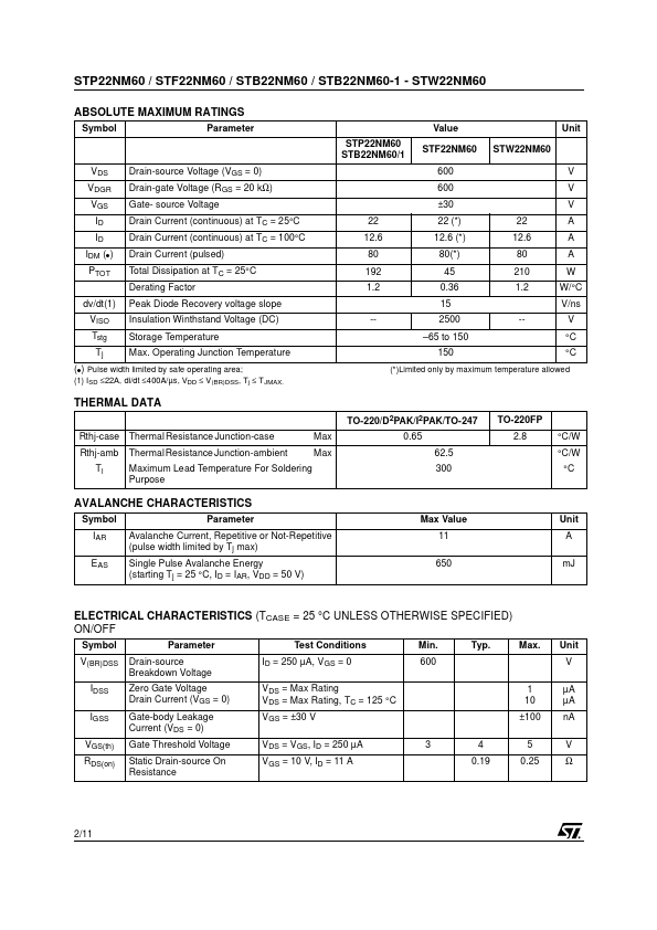
Symbol Parameter STP22NM60 STB22NM60/1 VDS VDGR VGS ID ID IDM ( ) PTOT dv/dt(1) VISO Tstg Tj Drain-source Voltage (VGS = 0) Drain-gate Voltage (RGS = 20 kΩ) Gate- source Voltage Drain Current (continuous) at TC = 25°C Drain Current (continuous) at TC = 100°C Drain Current (pulsed) Total Dissipation at TC = 25°C Derating Factor Peak Diode Recovery voltage slope Insulation Winthstand Voltage (DC) Storage Temperature Max.