STMicroelectronics STV160NF02LA
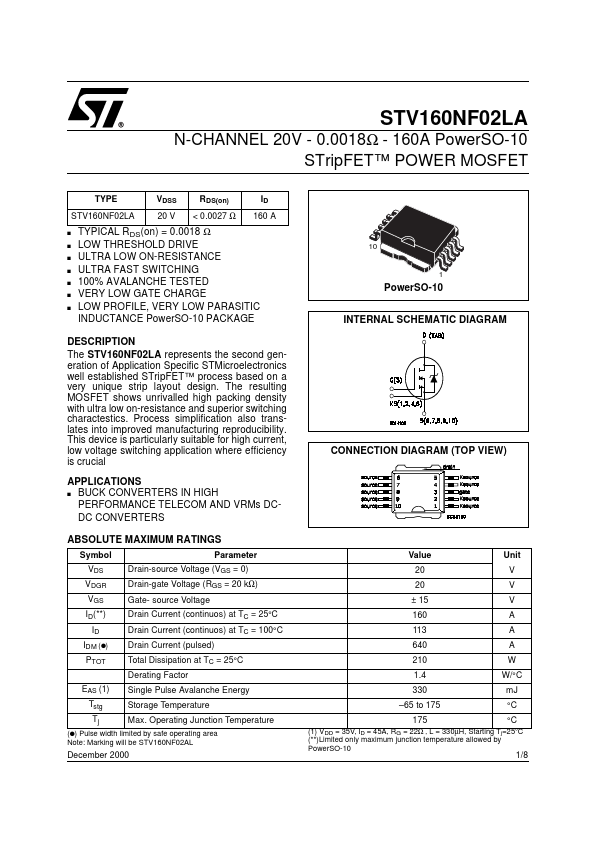
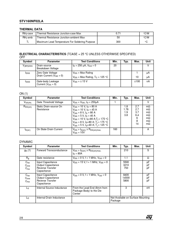
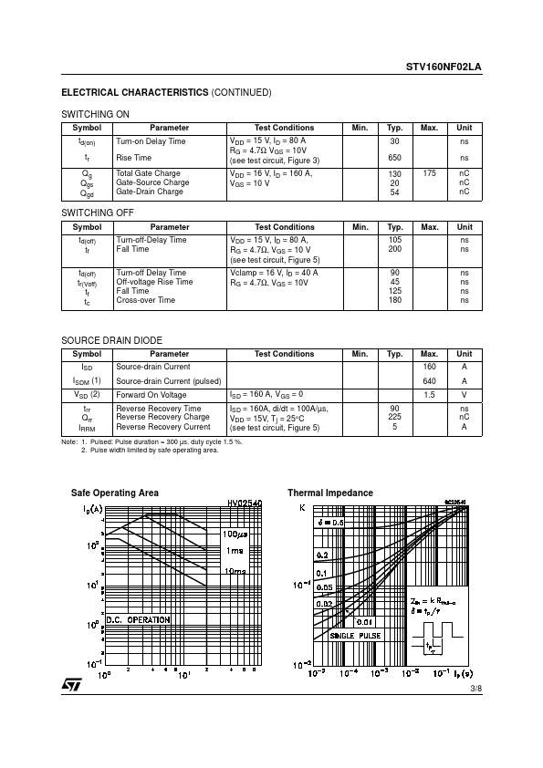
The STV160NF02LA represents the second generation of Application Specific STMicroelectronics well established STripFET™ process based on a very unique strip layout design. The resulting MOSFET shows unrivalled high packing density with ultra low on-resistance and superior switching charactestics. This device is particularly suitable for high current, low voltage switching application where efficiency is crucial APPLICATIONS s BUCK CONVERTERS IN HIGH PERFORMANCE TELECOM AND VRMs DCDC CONVERTERS ABSOLUTE MAXIMUM RATINGS Symbol VDS VDGR VGS ID(**) ID IDM (q) PTOT EAS (1) Tstg Tj Parameter Drain-source Voltage (VGS = 0) Drain-gate Voltage (RGS = 20 kΩ) Gate- source Voltage Drain Current (continuos) at TC = 25°C Drain Current (continuos) at TC = 100°C Drain Current (pulsed) Total Dissipation at TC = 25°C Derating Factor Single Pulse Avalanche Energy Storage Temperature Max.| Part No. | STV160NF02LA |
|---|---|
| Datasheet | STV160NF02LA Download |
| Manufacturer |  STMicroelectronics |
| Description | N-channel Power MOSFET |
| Buy | Stock & Price |