DESCRIPTION
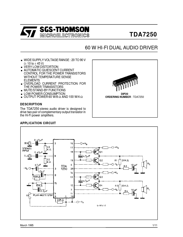
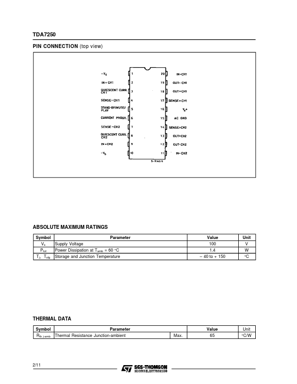
APPLICATION CIRCUIT March 1995 1/11 TDA7250 PIN CONNECTION (top view) ABSOLUTE MAXIMUM RATINGS
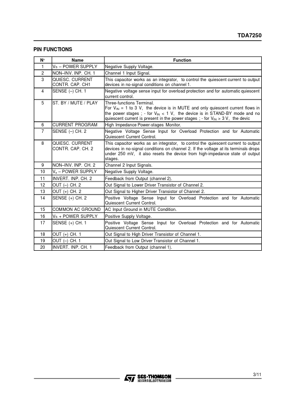
Symbol Vs Ptot Tj, Tstg Supply Voltage Power Dissipation at Tamb = 60 °C Storage and Junction Temperature Parameter Value 100 1.4 – 40 to + 150 Unit V W °C THERMAL DATA Symbol Rth j-amb Parameter Thermal Resistance Junction-ambient Max. Value 65 Unit °C/W 2/11 TDA7250 PIN FUNCTIONS N° 1 2 3 4 5 Name VS – POWER SUPPLY NON–INV. INP. CH. 1 QUIESC. CURRENT CONTR. CAP. CH1 SENSE (–) CH. 1 ST. BY / MUTE / PLAY Negative Supply Voltage. Channel 1 Input Signal. This capacitor works as an integrator, to control the quiescent current to output devices in no-signal conditions on channel 1. Negative voltage sense input for overload protection and for automatic quiescent current control. Three-functions Terminal. For VIN = 1 to 3 V, the device is in MUTE and only quiescent current flows in the power stages ; - for VIN < 1 V, the device is in STAND-BY mode and no quiescent current is present in the power stages ; - for VIN > 3 V, the devic High Impedance Power-stages Monitor. STMicroelectronics