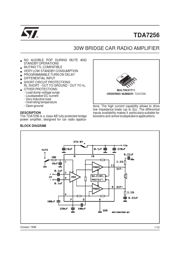
DESCRIPTION
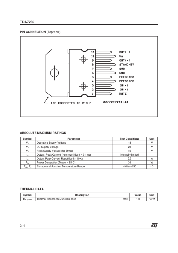
October 1998 1/10 This is advanced information on a new product now in development or undergoing evaluation. Details are subject to change without notice. TDA7256 PIN CONNECTION (Top view) ABSOLUTE MAXIMUM RATINGS
Symbol VS VS VS Io Io Ptot Tstg, TJ Operating Supply Voltage DC Supply Voltage Peak Supply Voltage (for 50ms) Output Peak Current (non repetiitive t = 0.1ms) Output Peak Current Repetitive f > 10Hz Power Dissipation (Tcase = 85°C) Storage and Junction Temperature Range Parameter Test Conditions 18 28 40 internally limited 5.5 36 -40 to +150 A W °C Unit V V V THERMAL DATA Symbol Rth j-case DESCRIPTION
Thermal Resistance Junction-case Max Value 1.8 Unit °C/W 2/10 TDA7256 ELECTRICAL CHARACTERISTICS
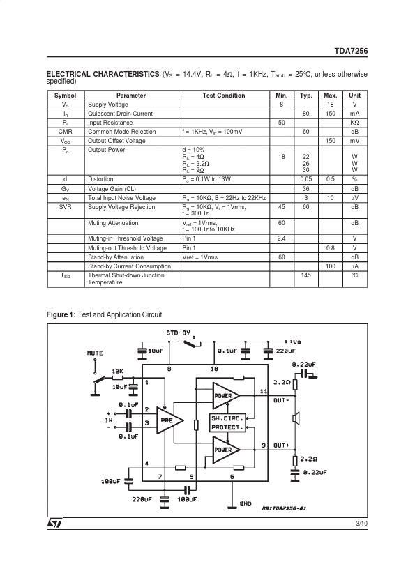
(VS = 14.4V, RL = 4Ω, f = 1KHz; Tamb = 25°C, unless otherwise specified) Symbol VS Iq Ri CMR VOS Po Parameter Supply Voltage Quiescent Drain Current Input Resistance Common Mode Rejection Output Offset Voltage Output Power d = 10% R L = 4Ω R L = 3.2Ω R L = 2Ω Po = 0.1W to... STMicroelectronics