DESCRIPTION
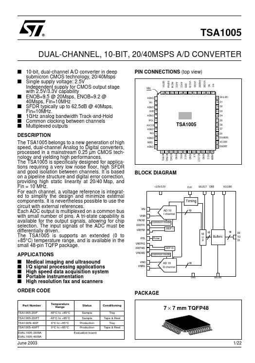
For each channel, a voltage reference is integrated to simplify the design and minimize external components. It is nevertheless possible to use the circuit with external references. Each ADC output is multiplexed on a common bus with small number of pins. A tri-state capability is available for the output signals, allowing for chip selection. The input signals of the ADC must be differentially driven. The TSA1005 is supports an extended (0 to +85°C) temperature range, and is available in the small 48-pin TQFP package. APPLICATIONS
BLOCK DIAGRAM +2.5V/3.3V CLK SELECT OEB REFPQ REFMQ INCMQ AGND AVCC DVCC Timing VINI VINBI VINCMI VREFPI VREFMI IPOL VREFPQ VREFMQ VINCMQ VINQ VINBQ REF Q REF I AD 10 I channel common mode 10 DGND CLK SELECT Polar. M U X DGND DVCC GNDBI VCCBE 10 10 Buffers D0 TO D9 common mode AD 10 Q channel 10 s s s s s Medical imaging and ultrasound I/Q signal processing applications High speed data acquisition system Portable instrumentation High resolution fa... STMicroelectronics