DESCRIPTION
APPLICATIONS
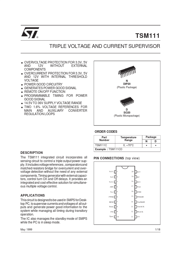
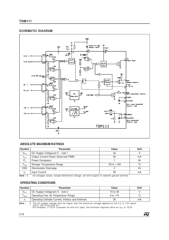
This circuit is designedto be used in SMPS forDesktop PC, to supervise currents and voltages of all outputs and generate power good information to the system while managing all timing during transitory operation. The IC also manages the standby mode of SMPS while the PC is in sleep mode. May 1999 PIN CONNECTIONS (top view) Vs33 Vs5 Vs12 ADJ Vcc P WM REM Tre m PG Tpor 1 2 3 4 5 6 7 8 9 10 20 19 18 17 16 15 14 13 12 11 Is33 Is5 Is12 Ts ur GND FbMAIN VrefMAIN VrefAUX FbAUX UV 1/18 TSM111 SCHEMATIC DIAGRAM ABSOLUTE MAXIMUM RATINGS
Symbol VCC Iout Pd Tstg ESD Iin Note : 1. Parameter DC Supply Voltage pin 5 - note 1 Output Current Power Good and PWM Power Dissipation Storage Temperature Range Electrostatic Discharge Input Current Value 44 30 1 -55 to +150 2 50 Unit V mA W o C kV mA Al l vol tages val ues, except dif ferenti al voltage, are w ith respect to netw ork ground terminal. OPERATING CONDITIONS Symbol VCC Toper Ik Note : Parameter DC Supply Voltage pin 5 - note 2 Operating Free Air Temperature Range Operating Cathode Current, Vrefaux and Vrefmain Value 15 to 36 0 to +70 30 Unit V o C mA 2. STMicroelectronics