DESCRIPTION
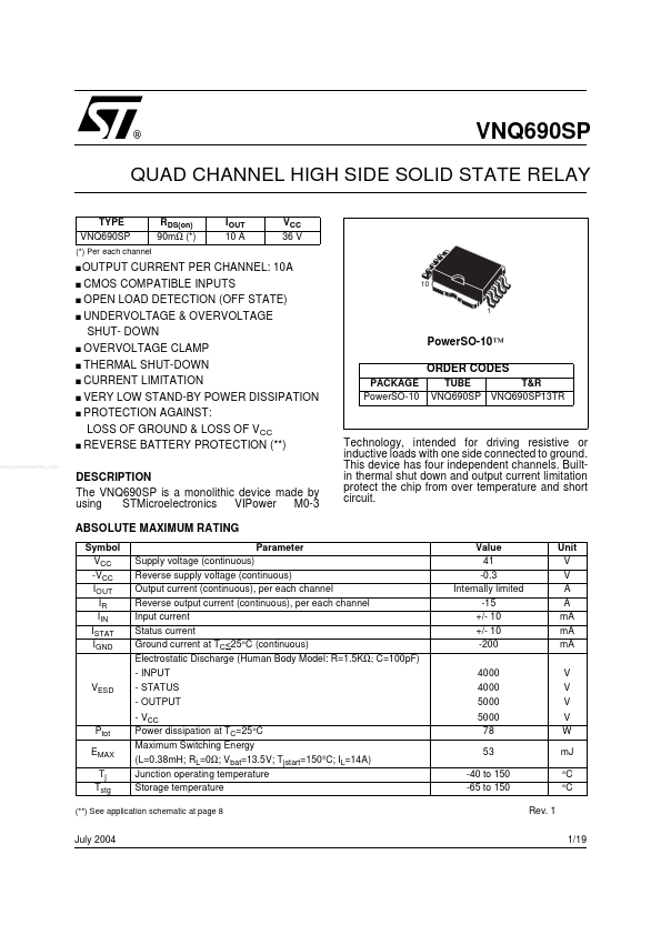
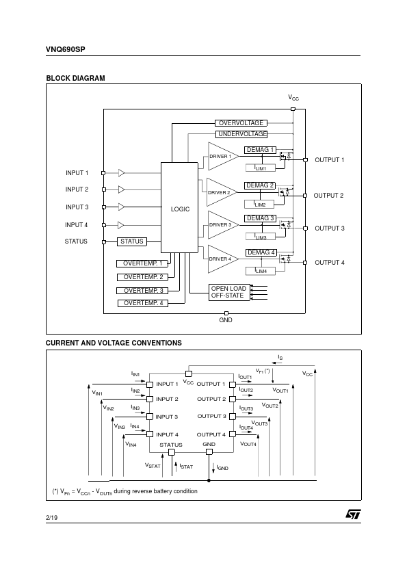
This device has four independent channels. Builtin thermal shut down and output current limitation protect the chip from over temperature and short circuit. Parameter Supply voltage (continuous) Reverse supply voltage (continuous) Output current (continuous), per each channel Reverse output current (continuous), per each channel Input current Status current Ground current at TC<25°C (continuous) Electrostatic Discharge (Human Body Model: R=1.5KΩ; C=100pF) - INPUT - STATUS - OUTPUT - VCC Power dissipation at TC=25°C Maximum Switching Energy (L=0.38mH; RL=0Ω; Vbat=13.5V; Tjstart=150ºC; IL=14A) Junction operating temperature Storage temperature Value 41 -0.3 Internally limited -15 +/- 10 +/- 10 -200 4000 4000 5000 5000 78 53 -40 to 150 -65 to 150 Rev. 1 Unit V V A A mA mA mA V V V V W mJ °C °C VESD Ptot EMAX Tj Tstg (**) See application schematic at page 8 July 2004 1/19 VNQ690SP BLOCK DIAGRAM VCC OVERVOLTAGE UNDERVOLTAGE DEMAG 1 DRIVER 1 OUTPUT 1 ILIM1 DEMAG 2 INPUT 1 INPUT 2 INPUT 3 INPUT 4 STATUS STATUS DRIVER 4 DRIVER 2 OUTPUT 2 ILIM2 DEMAG 3 LOGIC DRIVER 3 OUTPUT 3 ILIM3 DEMAG 4 OVERTEMP. STMicroelectronics