SPP3413W Overview
Description
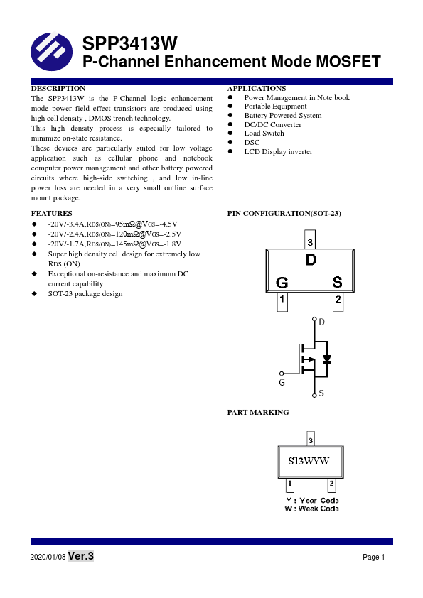
The SPP3413W is the P-Channel logic enhancement mode power field effect transistors are produced using high cell density , DMOS trench technology. This high density process is especially tailored to minimize on-state resistance.