SPP4925B
SPP4925B is P-Channel MOSFET manufactured by SYNC POWER.
P-Channel Enhancement Mode MOSFET
DESCRIPTION 
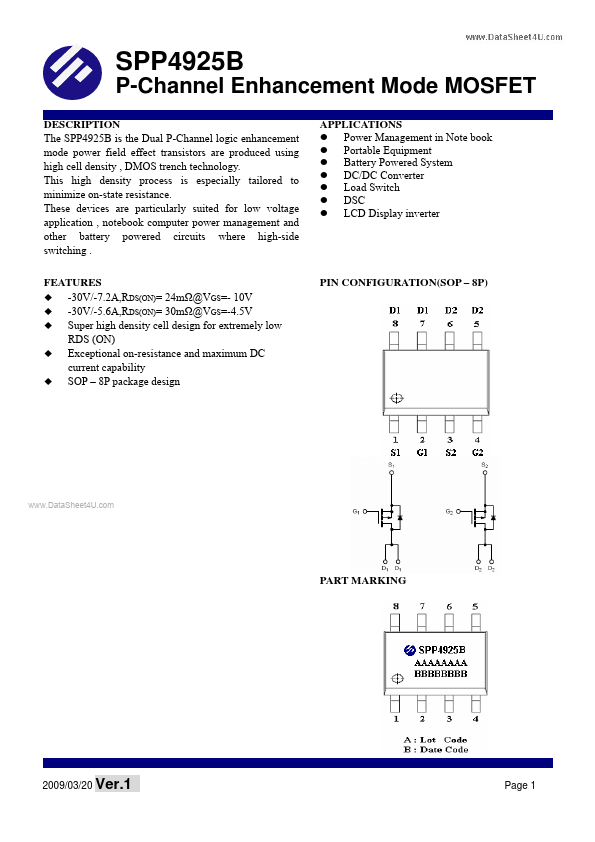
The SPP4925B is the Dual P-Channel logic enhancement mode power field effect transistors are produced using high cell density , DMOS trench technology. This high density process is especially tailored to minimize on-state resistance. These devices are particularly suited for low voltage application , notebook puter power management and other battery powered circuits where high-side switching . Features
-30V/-7.2A,RDS(ON)= 24mΩ@VGS=- 10V -30V/-5.6A,RDS(ON)= 30mΩ@VGS=-4.5V Super high density cell design for extremely low RDS (ON) Exceptional on-resistance and maximum DC current capability SOP
- 8P package design APPLICATIONS z Power Management in Note book z Portable Equipment z Battery Powered System z DC/DC Converter z Load Switch z DSC z LCD Display inverter
PIN CONFIGURATION(SOP
- 8P)
..
PART MARKING
2009/03/20 Ver.1
Page 1
P-Channel Enhancement Mode MOSFET
PIN DESCRIPTION
Pin 1 2 3 4 5 6 7 8
Symbol S1 G1 S2 G2 D2 D2 D1 D1
Description Source 1 Gate 1 Source 2 Gate 2 Drain 2 Drain 2 Drain 1 Drain 1
ORDERING INFORMATION Part Number SPP4925BS8RGB Package SOP- 8P Part Marking SPP4925B
※ SPP4925BS8RGB : 13” Tape Reel ; Halogen
- Free ; Pb
- Free
ABSOULTE MAXIMUM RATINGS (TA=25℃ Unless otherwise noted) Parameter
..
Symbol VDSS VGSS TA=25℃ TA=70℃ ID IDM IS TA=25℃ TA=70℃ PD TJ TSTG RθJA
Typical -30 ±20
Unit
Drain-Source Voltage Gate
- Source Voltage Continuous Drain Current(TJ=150℃) Pulsed Drain Current Continuous Source Current(Diode Conduction) Power Dissipation Operating Junction Temperature Storage Temperature Range Thermal Resistance-Junction to Ambient
V V A A A W ℃ ℃ ℃/W
-7.2 -5.6 -20 -2.3 2.8 1.8 -55/150 -55/150 70
2009/03/20 Ver.1
Page...