SP2702 Overview
Key Features
- Super high dense cell design for low RDS(ON)
- Rugged and reliable
- Suface Mount Package
| Part | SP2702 |
|---|---|
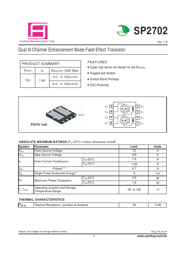
| Description | Dual N-Channel Enhancement Mode Field Effect Transistor |
| Category | Transistor |
| Manufacturer | SamHop Microelectronics |
| Size | 105.71 KB |
| Part Number | Manufacturer | Description |
|---|---|---|
| BDT88 | Inchange Semiconductor | Silicon PNP Power Transistor |
| KD333 | Tesla Elektronicke | Transistor |
| C828 | SEMTECH | NPN Silicon Transistor |