SamHop Microelectronics STA6610
Dual N-Channel Enhancement Mode Field Effect Transistor
| Part No. | STA6610 |
|---|---|
| Datasheet | STA6610 Download |
| Manufacturer |  SamHop Microelectronics |
| Description | Dual N-Channel Enhancement Mode Field Effect Transistor |
| Buy | Stock & Price |
ELECTRICAL CHARACTERISTICS
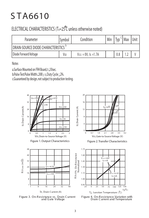
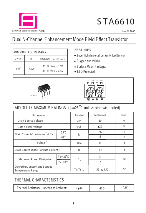
(TA=25 C unless otherwise noted) Parameter Diode Forward Voltage Symbol b Condition V GS = 0V, Is =1.7A Min Typ Max Unit 0.8 1.2 V C DRAIN-SOURCE DIODE CHARACTERISTICS VSD Notes a.Surface Mounted on FR4 Board,tІ10sec. b.Pulse Test:Pulse WidthІ300Ӵs,Duty Cycle І 2%. c.Guaranteed by design,not subject to production testing. 5 40 VGS=10V 32 VGS=4V VGS=4.5V 20 16 ID, Drain Current(A) ID, Drain Current (A) VGS=3.5V 24 Tj=125 C 12 -55 C 25 C 16 VGS=3V 8 VGS=2.5V 0 0 0.5 1 1.5 2 2.5 3 8 4 0 0 0.7 1.4 2.1 2.8 3.5 4.2 VDS, Drain-to-Source Voltage (V) VGS, Gate-to-Source Voltage (V) Figure 1. Output Characteristics 48 1.75 Figure 2. Transfer Characteristics R DS (ON) , On-R es is tance Normalized 40 1.60 1.45 1.30 1.15 1.00 0.85 -25 V G S =4.5V I D =5A V G S =10V I D =7A R DS (on) (m Ω) 32 24 16 8 1 V G S =4.5V V G S =10V 1 8 16 24 32 40 0 25 50 75 100 125 150 T j( C ) I D , Drain C urrent (A) T j, J unction T emperature ( C ) F igure 3. On-R es is tance vs . Drain C urrent and G ate V oltage F igure 4.