STS2307A
STS2307A is P-Channel Enhancement Mode Field Effect Transistor manufactured by SamHop Microelectronics.
S amHop Microelectronics C orp.
S T S 2307A
Dec 25 2004
P -C hannel E nhancement Mode Field E ffect Trans is tor
P R ODUC T S UMMAR Y
V DS S
-20V
F E AT UR E S
( m W ) Max
-2.8A
R DS (ON)
S uper high dense cell design for low R DS (ON ).
90 @ V G S = -4.5V 150 @ V G S = -2.5V
R ugged and reliable. S OT-23 package.
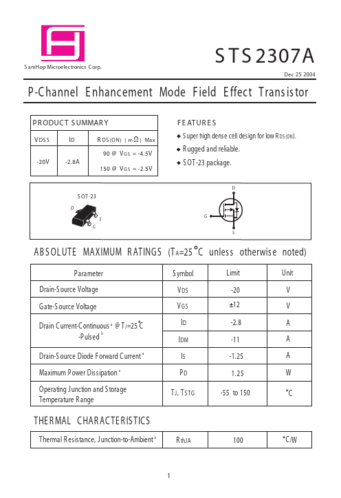
S OT-23
AB S OL UTE MAXIMUM R ATINGS (T A =25 C unles s otherwis e noted)
P arameter Drain-S ource Voltage Gate-S ource Voltage Drain C urrent-C ontinuous a @ T J =25 C b -P ulsed Drain-S ource Diode Forward C urrent a Maximum P ower Dissipation a Operating Junction and S torage Temperature R ange S ymbol V DS V GS ID IDM IS PD T J , T S TG Limit -20 12...