Samsung Semiconductor KM732V599L
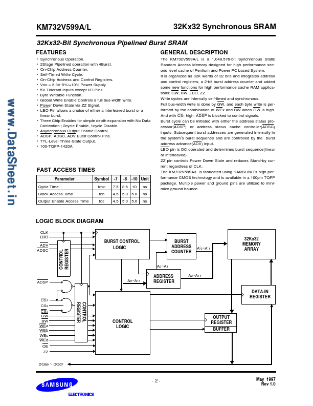
The KM732V599A/L is a 1,048,576-bit Synchronous Static Random Access Memory designed for high performance second level cache of Pentium and Power PC based System. It is organized as 32K words of 32 bits and integrates address and control registers, a 2-bit burst address counter and added some new functions for high performance cache RAM applications; GW, BW, LBO, ZZ.| Part No. | KM732V599L |
|---|---|
| Datasheet | KM732V599L Download |
| Manufacturer |  Samsung Semiconductor |
| Description | 32K X 32Bit Synchronous Pipelined Burst SRAM |
| Buy | Stock & Price |
FEATURES
●●
●
●
●
●
●
●
●
●
●
●
●
●
●
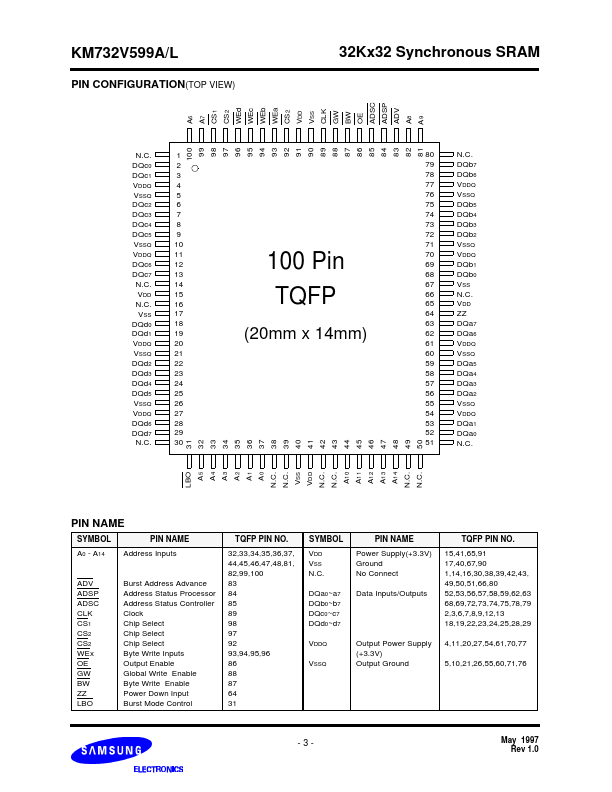
● Synchronous Operation. 2Stage Pipelined operation with 4Burst. On-Chip Address Counter. Self-Timed Write Cycle. On-Chip Address and Control Registers. VDD = 3.3V-5%/+10% Power Supply 5V Tolerant Inputs except I/O Pins Byte Writable Function. Global Write Enable Controls a full bus-width write. Power Down State via ZZ Signal. LBO Pin allows a choice of either a interleaved burst or a linear burst. Three Chip Enables for simple depth expansion with No Data Contention ; 2cycle Enable, 1cycle Disable. Asynchronous Output Enable Control. ADSP, ADSC, ADV Burst Control Pins. TTL-Level Three-State Output. 100-TQFP-1420A 32Kx32 Synchronous SRAM 32Kx32-Bit Synchronous Pipelined Burst SRAM
GENERAL DESCRIPTION
Write cycles are internally self-timed and synchronous. Full bus-width write is done by GW, and each byte write is performed by the combination of WEx and BW when GW is high. And with CS1 high, ADSP is blocked to control signals. Burst cycle can be initiated with either the address status processor(ADSP) or address status cache controller(ADSC) inputs.