K7D321874C Description
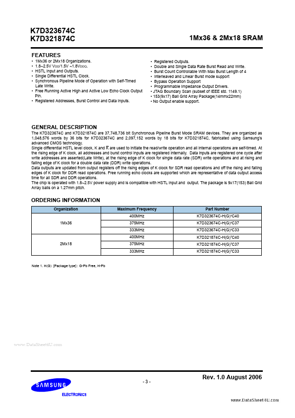
The K7D323674C and K7D321874C are 37,748,736 bit Synchronous Pipeline Burst Mode SRAM devices. Single differential HSTL level clock, K and K are used to initiate the read/write operation and all internal operations are self-timed. At the rising edge of K clock, all addresses and burst control inputs are registered internally.
K7D321874C Key Features
- 1Mx36 or 2Mx18 Organizations. 1.8~2.5V VDD/1.5V ~1.8VDDQ. HSTL Input and Outputs. Single Differential HSTL Clock. Synchr
- Free Running Active High and Active Low Echo Clock Output Pin
- Registered Addresses, Burst Control and Data Inputs
- Registered Outputs
- Double and Single Data Rate Burst Read and Write
- Burst Count Controllable With Max Burst Length of 4
- Interleaved and Linear Burst mode support
- Bypass Operation Support
- Programmable Impedance Output Drivers
- JTAG Boundary Scan (subset of IEEE std. 1149.1)
K7D321874C Applications
- Samsung Electronics reserves the right to change products or specification without notice