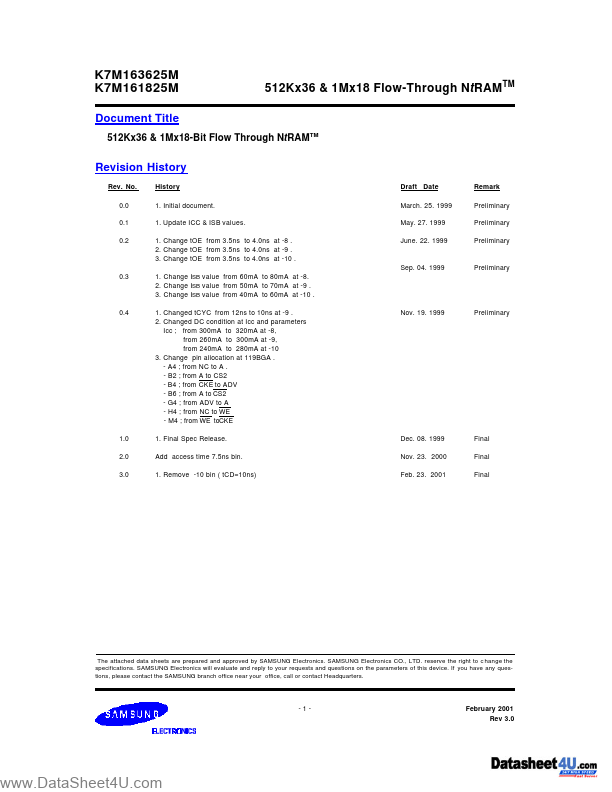
K7M163625M
K7M163625M is 512Kx36 & 1Mx18 Flow-Through NtRAM manufactured by Samsung Semiconductor.
- Part of the K7M161825M comparator family.
- Part of the K7M161825M comparator family.
FEATURES
- 3.3V+0.165V/-0.165V Power Supply.
- I/O Supply Voltage 3.3V+0.165V/-0.165V for 3.3V I/O or 2.5V+0.4V/-0.125V for 2.5V I/O
- Byte Writable Function.
- Enable clock and suspend operation.
- Single READ/WRITE control pin.
- Self-Timed Write Cycle.
- Three Chip Enable for simple depth expansion with no data contention .
- A interleaved burst or a linear burst mode.
- Asynchronous output enable control.
- Power Down mode.
- TTL-Level Three-State Outputs.
- 100-TQFP-1420A /119BGA(7x17 Ball Grid Array Package).
GENERAL DESCRIPTION
The K7M163625M and K7M161825M are 18,874,368-bits Synchronous Static SRAMs. The N t RAM TM , or No Turnaround Random Access Memory utilizes all bandwidth in any bination of operating cycles. Address, data inputs, and all control signals except output enable and linear burst order are synchronized to input clock. Burst order control must be tied "High or Low". Asynchronous inputs include the sleep mode enable(ZZ). Output Enable controls the outputs at any given time. Write cycles are internally self-timed and initiated by the rising edge of the clock input. This feature eliminates plex off-chip write pulse generation and provides increased timing flexibility for ining signals. For read cycles, Flow-Through...