K7R161884B Description
Change the Boundary scan exit order. Correct the Overshoot and Undershoot timing diagram. Change JTAG Block diagram.
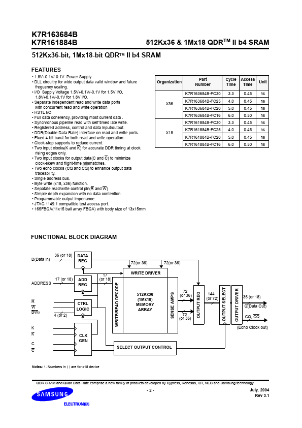
K7R161884B Key Features
- 1.8V+0.1V/-0.1V Power Supply
- DLL circuitry for wide output data valid window and future freguency scaling
- I/O Supply Voltage 1.5V+0.1V/-0.1V for 1.5V I/O, 1.8V+0.1V/-0.1V for 1.8V I/O
- Separate independent read and write data ports with concurrent read and write operation
- HSTL I/O
- Full data coherency, providing most current data
- Synchronous pipeline read with self timed late write
- Registered address, control and data input/output
- DDR(Double Data Rate) Interface on read and write ports
- Fixed 4-bit burst for both read and write operation