Datasheet4U Logo Datasheet4U.com

K8S6415ETB - (K8S6415ExB) 64M Bit Multi Bank NOR Flash Memory

Download the K8S6415ETB datasheet PDF. This datasheet also covers the K8S6415EBB variant, as both devices belong to the same (k8s6415exb) 64m bit multi bank nor flash memory family and are provided as variant models within a single manufacturer datasheet.

General Description

is added January 09,2006 www.DataSheet4U.com 1.1 1 Revision 1.1 January, 2006 K8S6415ET(B)B

Key Features

  • Single Voltage, 1.7V to 1.95V for Read and Write operations.
  • Organization - 4,194,304 x 16 bit ( Word Mode Only).
  • Multiplexed Data and Address for reduction of interconnections - A/DQ0 ~ A/DQ15.
  • Read While Program/Erase Operation.
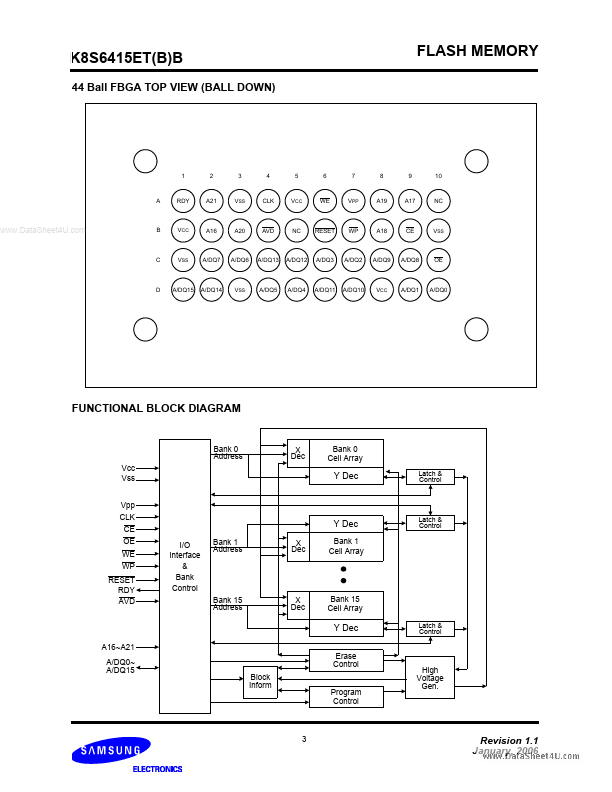
  • Multiple Bank Architecture - 16 Banks (4Mb Partition).
  • OTP Block : Extra 256Byte block.
  • Read Access Time (@ CL=30pF) - Asynchronous Random Access Time : www. DataSheet4U. com 90ns (54MHz) / 80ns (66MHz) - Sy.

📥 Download Datasheet

Note: The manufacturer provides a single datasheet file (K8S6415EBB_Samsungsemiconductor.pdf) that lists specifications for multiple related part numbers.

Full PDF Text Transcription for K8S6415ETB (Reference)

Note: Below is a high-fidelity text extraction (approx. 800 characters) for K8S6415ETB. For precise diagrams, and layout, please refer to the original PDF.

K8S6415ET(B)B FLASH MEMORY Document Title 64M Bit (4M x16) Muxed Burst , Multi Bank NOR Flash Memory Revision History Revision No. History 0.0 1.0 Initial Issue Draft Dat...

View more extracted text
Revision History Revision No. History 0.0 1.0 Initial Issue Draft Date October 20, 2004 Remark Revision March 22, 2005 - Specification finalized - Add the requirement and note of Quadruple word program operation Bottom boot block description is added January 09,2006 www.DataSheet4U.com 1.1 1 Revision 1.1 January, 2006 K8S6415ET(B)B FEATURES • Single Voltage, 1.7V to 1.