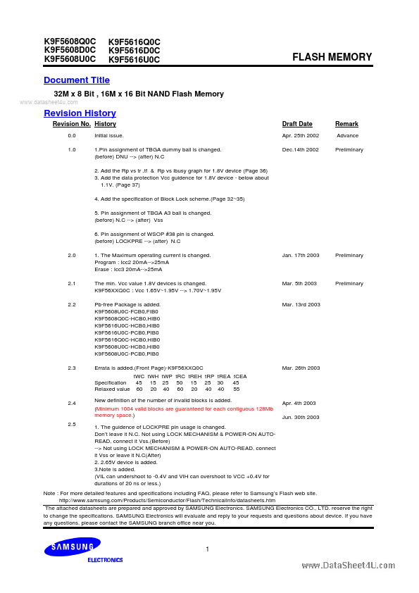
Datasheet4U Logo Datasheet4U.com

K9F5608QOC - (K9F5608xOC / K9F5616xOC) 32M x 8 Bit 16M x 16 Bit NAND Flash Memory

This page provides the datasheet information for the K9F5608QOC, a member of the K9F5608UOC (K9F5608xOC / K9F5616xOC) 32M x 8 Bit 16M x 16 Bit NAND Flash Memory family.

Datasheet Summary

Description

Offered in 32Mx8bit or 16Mx16bit, the K9F56XXX0C is 256M bit with spare 8M bit capacity.

The device is offered in 1.8V, 2.65V, 3.3V Vcc.

Its NAND cell provides the most cost-effective solutIon for the solid state mass storage market.

Features

  • and specifications including FAQ, please refer to Samsung’ s Flash web site. http://www. samsung. com/Products/Semiconductor/Flash/TechnicalInfo/datasheets. htm The attached datasheets are prepared and approved by.

📥 Download Datasheet

Datasheet preview – K9F5608QOC

Datasheet Details

Part number K9F5608QOC
Manufacturer Samsung semiconductor
File Size 736.83 KB
Description (K9F5608xOC / K9F5616xOC) 32M x 8 Bit 16M x 16 Bit NAND Flash Memory
Datasheet download datasheet K9F5608QOC Datasheet
Additional preview pages of the K9F5608QOC datasheet.
Other Datasheets by Samsung semiconductor

Full PDF Text Transcription

Click to expand full text
K9F5608Q0C K9F5608D0C K9F5608U0C K9F5616Q0C K9F5616D0C K9F5616U0C FLASH MEMORY Document Title 32M x 8 Bit , 16M x 16 Bit NAND Flash Memory www.datasheet4u.com Revision History Revision No. History 0.0 1.0 Initial issue. 1.Pin assignment of TBGA dummy ball is changed. (before) DNU --> (after) N.C 2. Add the Rp vs tr ,tf & Rp vs ibusy graph for 1.8V device (Page 36) 3. Add the data protection Vcc guidence for 1.8V device - below about 1.1V. (Page 37) 4. Add the specification of Block Lock scheme.(Page 32~35) 5. Pin assignment of TBGA A3 ball is changed. (before) N.C --> (after) Vss 6. Pin assignment of WSOP #38 pin is changed. (before) LOCKPRE --> (after) N.C 2.0 1. The Maximum operating current is changed. Program : Icc2 20mA-->25mA Erase : Icc3 20mA-->25mA The min. Vcc value 1.
Published: |