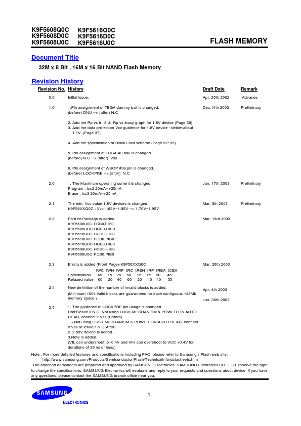
| Part | K9F5608Q0C |
|---|---|
| Description | NAND Flash Memory |
| Manufacturer | Samsung Semiconductor |
| Size | 674.30 KB |
Pricing from 8.6908 USD, available from Win Source and ICPartonline.
Price & Availability
| Seller | Inventory | Price Breaks | Buy |
|---|---|---|---|
| Win Source | 5 | 7+ : 8.6908 USD 17+ : 7.131 USD 26+ : 6.9082 USD 35+ : 6.6853 USD |
View Offer |
| ICPartonline | 10421 | 1+ : 1.58 USD 10+ : 1.501 USD 100+ : 1.422 USD 1000+ : 1.343 USD |
View Offer |
Related Datasheets
| Part Number | Manufacturer | Description |
|---|---|---|
| K9F5608U0B-DCB0 | Samsung Semiconductor | 32M x 8 Bit / 16M x 16 Bit NAND Flash Memory |
| K9F5608U0B-PCB0 | Samsung Semiconductor | 32M x 8 Bit / 16M x 16 Bit NAND Flash Memory |
| K9F5608U0D | Samsung Semiconductor | 32M x 8 Bit NAND Flash Memory |
| K9F5608U0A | Samsung Semiconductor | 32M x 8 Bit NAND Flash Memory |
| K9F5608U0C-V | Samsung Semiconductor | 512Mb/256Mb 1.8V NAND Flash Errata |

