K9F5608U0M-YCB0
K9F5608U0M-YCB0 is 32M x 8 Bit NAND Flash Memory manufactured by Samsung Semiconductor.
K9F5608U0M-YCB0,K9F5608U0M-YIB0
Document Title
32M x 8 Bit NAND Flash Memory
FLASH MEMORY
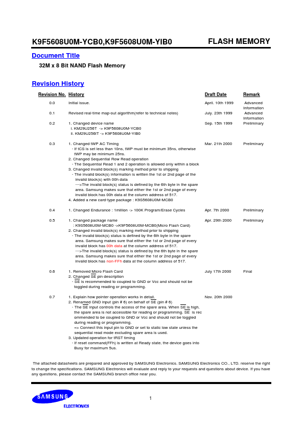
Revision History
Revision No. History
0.0 0.1 0.2 Initial issue. Revised real-time map-out algorithm(refer to technical notes) 1. Changed device name i. KM29U256T -> K9F5608U0M-YCB0 ii. KM29U256IT -> K9F5608U0M-YIB0 1. Changed tWP AC Timing
- If tCS is set less than 10ns, tWP must be minimum 35ns, otherwise tWP may be minimum 25ns. 2. Changed Sequential Row Read operation
- The Sequential Read 1 and 2 operation is allowed only within a block 3. Changed invalid block(s) marking method prior to shipping
- The invalid block(s) information is written the 1st or 2nd page of the invalid block(s) with 00h...