K9F8008W0M-TCB0
K9F8008W0M-TCB0 is 1M x 8 bit NAND Flash Memory manufactured by Samsung Semiconductor.
K9F8008W0M-TCB0, K9F8008W0M-TIB0
Document Title
1M x 8 bit NAND Flash Memory
FLASH MEMORY
Revision History
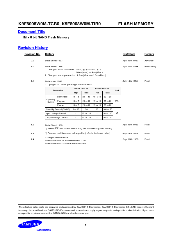
Revision No.
0.0 1.0
History
Data Sheet 1997 Data Sheet 1998 1. Changed tBERS parameter : 5ms(Typ.) → 2ms(Typ.) 10ms(Max.) → 4ms(Max.) 2. Changed tPROG parameter : 1.5ms(Max.) → 1.0ms(Max.) Data sheet 1998 1. Cjanged DC and Operating Characteristics
Parameter Burst Read Operating Current Program Eraase Stand-by Current (CMOS) Input Leakage Current Output Leakage Current Vcc=2.7V~3.6V Typ 10 → 5 10 → 5 10 → 5 5 → 10 Max 20 → 10 20 → 10 20 → 10 50 10 → ±10 10 → ±10 Vcc=3.6V~5.5V Typ 15 → 10 15 → 10 15 → 10 10 Max 30 → 20 30 → 20 30 → 20 100 → 50 10 → ±10 10 → ±10 µA mA Unit
Draft...