KFH1G16Q2M
KFH1G16Q2M is FLASH MEMORY manufactured by Samsung Semiconductor.
One NAND512/One NAND1GDDP
FLASH MEMORY
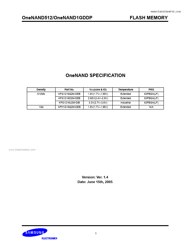
One NAND SPECIFICATION
Density 512Mb Part No. KFG1216Q2M-DEB KFG1216D2M-DEB KFG1216U2M-DIB 1Gb KFH1G16Q2M-DEB VCC(core & IO) 1.8V(1.7V~1.95V) 2.65V(2.4V~2.9V) 3.3V(2.7V~3.6V) 1.8V(1.7V~1.95V) Temperature Extended Extended Industrial Extended PKG 63FBGA(LF) 63FBGA(LF) 63FBGA(LF) N/A
..
Version: Ver. 1.4 Date: June 15th, 2005
One NAND512/One NAND1GDDP
FLASH MEMORY
INFORMATION IN THIS DOCUMENT IS PROVIDED IN RELATION TO SAMSUNG PRODUCTS, AND IS SUBJECT TO CHANGE WITHOUT NOTICE. NOTHING IN THIS DOCUMENT SHALL BE CONSTRUED AS GRANTING ANY LICENSE, EXPRESS OR IMPLIED, BY ESTOPPEL OR OTHERWISE, TO ANY INTELLECTUAL PROPERTY RIGHTS IN SAMSUNG PRODUCTS OR TECHNOLOGY. ALL INFORMATION IN THIS DOCUMENT IS PROVIDED .. ON AS "AS IS" BASIS WITHOUT GUARANTEE OR WARRANTY OF ANY KIND. 1. For updates or additional information about Samsung products, contact your nearest Samsung office. 2. Samsung products are not intended for use in life support, critical care, medical, safety equipment, or similar applications where Product failure could result in loss of life or personal or physical harm, or any military or defense application, or any governmental procurement to which special terms or provisions may apply. One NAND™‚ is a trademark of Samsung Electronics pany, Ltd. Other names and brands may be claimed as the property of their rightful owners. Copyright © 2005, Samsung Electronics pany, Ltd
One NAND512/One NAND1GDDP
Document Title
One NAND
FLASH MEMORY
Revision History
Revision No. History
0.0 0.0.1 Initial issue.
Draft Date
Jan. 07, 2004
Remark
Preliminary Preliminary
1. Add the "Invalid block management" and "Error management in read and Jan. 29, 2004 write operation" 2. Add the restriction in addressing for program operation. 3. Add the asynchronous write and latched asynchronous write mode timing diagram. 4.Define new parameters in asynchronous write mode. -t CH1 : 10ns, t CH2 : 0ns 1. Add the dual operation diagram. 2. Add the...