Datasheet Summary
64MB, 128MB, 256MB Unbuffered DIMM
SDRAM
SDRAM Unbuffered Module
168pin Unbuffered Module based on 128Mb E-die 62/72-bit Non ECC/ECC
Revision 1.3 February. 2004
Rev. 1.3 February 2004
64MB, 128MB, 256MB Unbuffered DIMM
Revision History
Revision 1.0 (November., 2002)
- First release Revision 1.1 (May, 2003)
- Merged Spec. Revision 1.2 (June, 2003)
- Correct Typo. Revision 1.3 (February, 2004)
- Correct Typo.
SDRAM
Rev. 1.3 February 2004
64MB, 128MB, 256MB Unbuffered DIMM
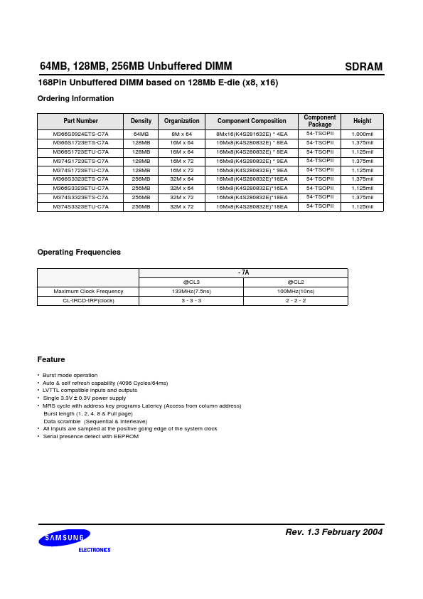
168Pin Unbuffered DIMM based on 128Mb E-die (x8, x16)
Ordering Information
Part Number M366S0924ETS-C7A M366S1723ETS-C7A M366S1723ETU-C7A M374S1723ETS-C7A M374S1723ETU-C7A M366S3323ETS-C7A M366S3323ETU-C7A...