Datasheet4U Logo Datasheet4U.com

S1M8662A - CDMA/PCS/GPS Triple Mode IF/ baseband IC

General Description

Pin No 1 2 3 4 5 6 7 8 9 10 11 12 13 Symbol VDDD VDDA RAGC_CONT GRX_IF1 GRX_IF2 CRX_IF1 CRX_IF2 VDDA TCXO_out VDDA VDDA Q_OFS I_OFS P DO P P AI I/O P P AI AI Power for the digital logic.

Power input terminal for the analog circuit.

AGC gain control input.

Key Features

  • Cellular CDMA/PCS/GPS Triple Mode AGC input signal range : 90dB QPSK Baseband Converter Built-in I ,Q Baseband signal extractor LPF Built-in 4-bit ADC for converting I and Q CDMA analog baseband signals to digital baseband signals Built-in VCO for baseband conversion Built-in Modem PDM control circuit to compensate the I and Q offsets Built-in TCXO output ON/OFF 3-Line Serial Port Interf.

📥 Download Datasheet

Full PDF Text Transcription (Reference)

The following content is an automatically extracted verbatim text from the original manufacturer datasheet and is provided for reference purposes only.

View original datasheet text
RX IF/BBA WITH GPS S1M8662A (Preliminary) INTRODUCTION 
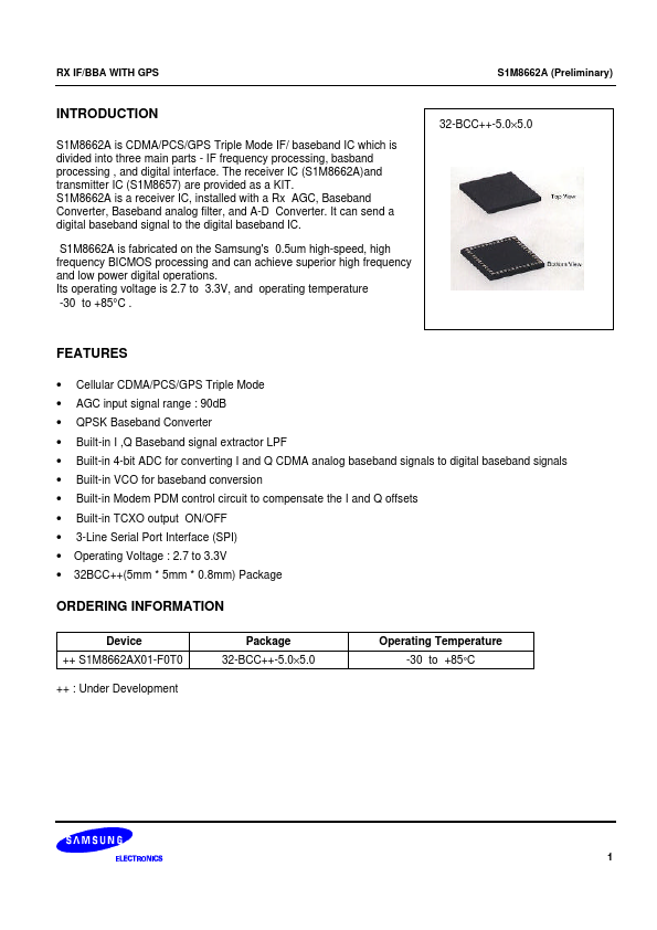
S1M8662A is CDMA/PCS/GPS Triple Mode IF/ baseband IC which is divided into three main parts - IF frequency processing, basband processing , and digital interface. The receiver IC (S1M8662A)and transmitter IC (S1M8657) are provided as a KIT. S1M8662A is a receiver IC, installed with a Rx AGC, Baseband Converter, Baseband analog filter, and A-D Converter. It can send a digital baseband signal to the digital baseband IC. S1M8662A is fabricated on the Samsung's 0.5um high-speed, high frequency BICMOS processing and can achieve superior high frequency and low power digital operations. Its operating voltage is 2.7 to 3.3V, and operating temperature -30 to +85°C . 32-BCC++-5.0×5.