Datasheet4U Logo Datasheet4U.com

K7D801871B - SRAM

This page provides the datasheet information for the K7D801871B, a member of the K7D803671B SRAM family.

Datasheet Summary

Description

Pin Name K, K SA SA0, SA1 DQ VDD VDDQ VREF B1 B2 B3 Pin Description Differential Clocks Synchronous Address Input Synchronous Burst Address Input (SA0 = LSB) Synchronous Data I/O Core Power Supply Output Power Supply HSTL Input Reference Voltage Load External Address Burst R/W Enable Single/Double

Features

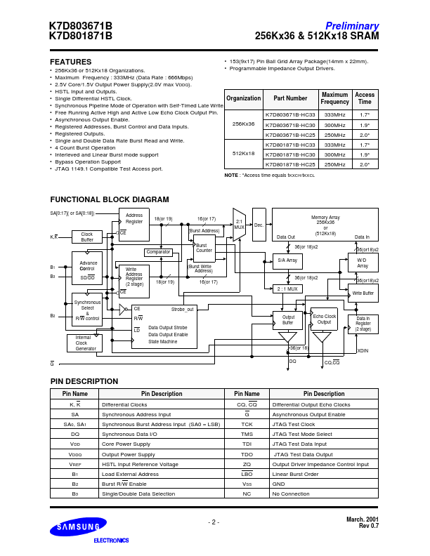
  • 256Kx36 or 512Kx18 Organizations.
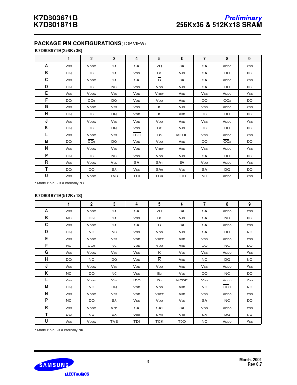
  • 153(9x17) Pin Ball Grid Array Package(14mm x 22mm).
  • Programmable Impedance Output Drivers.
  • Maximum Frequency : 333MHz (Data Rate : 666Mbps).
  • 2.5V Core/1.5V Output Power Supply(2.0V max VDDQ).
  • HSTL Input and Outputs.
  • Single Differential HSTL Clock. Organization.
  • Synchronous Pipeline Mode of Operation with Self-Timed Late Write. Part Number Maximum Access Frequency Time.

📥 Download Datasheet

Datasheet preview – K7D801871B

Datasheet Details

Part number K7D801871B
Manufacturer Samsung
File Size 299.69 KB
Description SRAM
Datasheet download datasheet K7D801871B Datasheet
Additional preview pages of the K7D801871B datasheet.
Other Datasheets by Samsung

Full PDF Text Transcription

Click to expand full text
K7D803671B K7D801871B Preliminary 256Kx36 & 512Kx18 SRAM Document Title 8M DDR SYNCHRONOUS SRAM Revision History Rev No. Rev. 0.0 History -Initial document. Rev. 0.1 -ZQ tolerance changed from 10% to 15% Rev. 0.2 -Stop Clock Standby Current condition changed from VIN=VDD-0.2V or 0.2V fixed to VIN=VIH or VIH Rev. 0.3 -VDDQ Max. changed to 2.0V SA0, SA1 defined for Boundary Scan Order Rev. 0.5 -Deleted -HC16 part(Part Number, Idd, AC Characterisctics) Rev. 0.6 - Absolute Maximum ratings VDDQ changed from 3.13V to 2.825V Rev. 0.7 - LBO input level changed from High/Low to VDD/VSS - Stop Clock Standby Current condition changed from K=Low, K=High to K=Low, K=Low - tCHQV/tCLQV changed from 0.1ns to 0.2ns for -33 part from 0.1ns to 0.2ns for -30 part from 0.1ns to 0.
Published: |