Datasheet4U Logo Datasheet4U.com

LC89950 - 1H Delay Line

Datasheet Summary

Features

  • 5-V single-voltage power supply.
  • Two input and output systems, one each for R-Y and BY signals.
  • Takes a sandcastle pulse (SCP) as the input clock, and converts that to a burst gate pulse (BGP) signal internally.
  • Generates the CCD drive pulses (4 MHz) from the input clock using a PLL circuit.
  • Uses BGP as clamp pulses and clamps the no signal section (back porch) once every horizontal scan period.
  • The output signal is in-phase with the inpu.

📥 Download Datasheet

Datasheet preview – LC89950

Datasheet Details

Part number LC89950
Manufacturer Sanyo
File Size 98.98 KB
Description 1H Delay Line
Datasheet download datasheet LC89950 Datasheet
Additional preview pages of the LC89950 datasheet.
Other Datasheets by Sanyo

Full PDF Text Transcription

Click to expand full text
Ordering number : EN*5440 MOS LSI LC89950 1H Delay Line for PAL Systems Preliminary Overview The LC89950 is an IC that provides 1H delay processing for color difference signals used in PAL and SECAM format TV. The LC89950 has two CCD systems, one for the R-Y and one for the B-Y signal, and drives these CCDs with a 4-MHz clock generated within the IC. It uses a sandcastle-shaped three-value input clock with a 1 H (64 µs) period. • Auto-bias and input clamping circuits • 4-MHz output circuit 
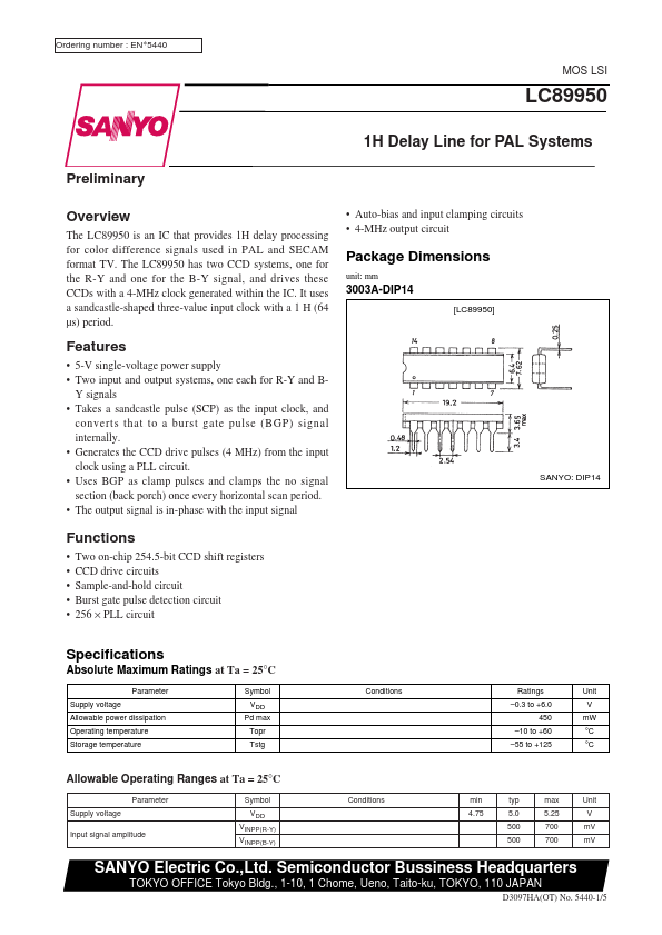
Package Dimensions unit: mm 3003A-DIP14 [LC89950] Features • 5-V single-voltage power supply • Two input and output systems, one each for R-Y and BY signals • Takes a sandcastle pulse (SCP) as the input clock, and converts that to a burst gate pulse (BGP) signal internally.
Published: |