2N3233 Overview
Key Specifications
Max Operating Temp: 175 °C
Description
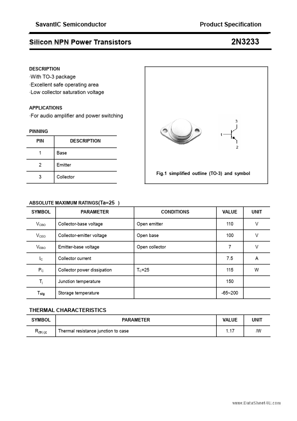
With TO-3 package - Excellent safe operating area - Low collector saturation voltage.
| Part | 2N3233 |
|---|---|
| Description | Silicon NPN Power Transistors |
| Category | Transistor |
| Manufacturer | SavantIC |
| Size | 134.44 KB |
Max Operating Temp: 175 °C
With TO-3 package - Excellent safe operating area - Low collector saturation voltage.
| Seller | Inventory | Price Breaks | Buy |
|---|---|---|---|
| No distributor offers were returned for this part. | |||
| Part Number | Manufacturer | Description |
|---|---|---|
| 2N3236 | Inchange Semiconductor | Silicon NPN Power Transistor |
| 2N3239 | Inchange Semiconductor | Silicon NPN Power Transistor |
| 2N3235 | Westinghouse | Silicon Power Transistors |
| 2N3238 | Inchange Semiconductor | Silicon NPN Power Transistor |
| 2N3235 | Motorola Semiconductor | NPN silicon power transistors |