2SA1180
Overview
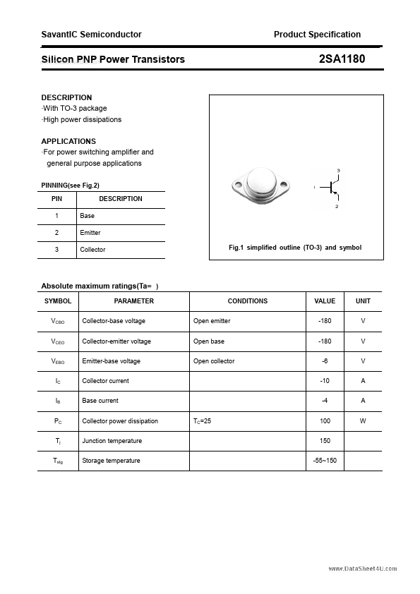
SavantIC Semiconductor Product Specification Silicon PNP Power Transistors 2SA1180 DESCRIPTION ·With TO-3 package ·High power dissipations APPLICATIONS ·For power switching amplifier and general ...
| Part | 2SA1180 |
|---|---|
| Description | SILICON POWER TRANSISTOR |
| Category | Transistor |
| Manufacturer | SavantIC |
| Size | 134.62 KB |
SavantIC Semiconductor Product Specification Silicon PNP Power Transistors 2SA1180 DESCRIPTION ·With TO-3 package ·High power dissipations APPLICATIONS ·For power switching amplifier and general ...
| Part Number | Manufacturer | Description |
|---|---|---|
| 2SA1182 | Kexin Semiconductor | PNP Transistors |