2SB713
2SB713 is SILICON POWER TRANSISTOR manufactured by SavantIC.
DESCRIPTION
- With TO-3PN package
- Wide area of safe operation
- Excellent good linearity of h FE APPLICATIONS
- For high power amplifier applications
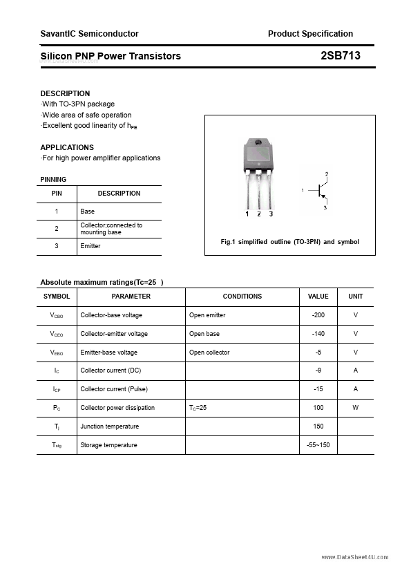
PINNING PIN 1 2 3 Base Collector;connected to mounting base Emitter Fig.1 simplified outline (TO-3PN) and symbol DESCRIPTION
Absolute maximum ratings(Tc=25 )
SYMBOL VCBO VCEO VEBO IC ICP PC Tj Tstg PARAMETER Collector-base voltage Collector-emitter voltage Emitter-base voltage Collector current (DC) Collector current (Pulse) Collector power dissipation Junction temperature Storage temperature TC=25 CONDITIONS Open emitter Open base Open collector VALUE -200 -140 -5 -9 -15 100 150 -55~150 UNIT V V V A A W
Savant IC Semiconductor
..
Product Specification
Silicon PNP Power Transistors
CHARACTERISTICS
Tj=25 unless otherwise specified PARAMETER Collector-emitter saturation voltage Base-emitter on voltage Collector cut-off current Emitter cut-off current DC current gain DC current gain DC current gain Transition frequency Collector output capacitance CONDITIONS IC=-7A; IB=-0.7A IC=-7A;VCE=-5V VCB=-140V; IE=0 VEB=-3V; IC=0 IC=-20m A ; VCE=-5V IC=-1A ; VCE=-5V IC=-7A ; VCE=-5V IC=-0.5A ; VCE=-5V f=1MHz;VCB=-10V 20 40 15 7 220 MIN TYP.
SYMBOL VCEsat VBE ICBO IEBO h FE-1 h FE-2 h FE-3 f T COB
MAX -2.0 -1.8 -50 -50
UNIT V V µA µA
MHz p F h FE-2 Classifications R 40-80 Q 60-120 P 100-200
Savant IC Semiconductor
..
Product Specification
Silicon PNP Power Transistors
PACKAGE OUTLINE
Fig.2 outline...