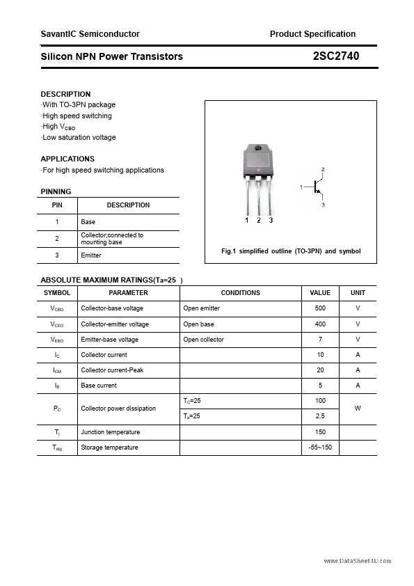
With TO-3PN package
High speed switching
High VCBO
Low saturation voltage APPLICATIONS
For high speed switching applications PINNING
PIN 1 2 3 Base Collector;connected to mounting base Emitter Fig.1 simplified outline (TO-3PN) and symbol DESCRIPTION
ABSOLUTE MAXIMUM RATINGS
The following content is an automatically extracted verbatim text
from the original manufacturer datasheet and is provided for reference purposes only.
View original datasheet text
SavantIC Semiconductor
www.DataSheet4U.com
Product Specification
Silicon NPN Power Transistors
2SC2740
DESCRIPTION ·With TO-3PN package ·High speed switching ·High VCBO ·Low saturation voltage APPLICATIONS ·For high speed switching applications PINNING
PIN 1 2 3 Base Collector;connected to mounting base Emitter Fig.1 simplified outline (TO-3PN) and symbol DESCRIPTION
ABSOLUTE MAXIMUM RATINGS(Ta=25 )
SYMBOL VCBO VCEO VEBO IC ICM IB PARAMETER Collector-base voltage Collector-emitter voltage Emitter-base voltage Collector current Collector current-Peak Base current TC=25 PC Collector power dissipation Ta=25 Tj Tstg Junction temperature Storage temperature 2.