
Datasheet Summary
SavantIC Semiconductor
..
Product Specification
Silicon NPN Power Transistors
DESCRIPTION
- With TO-3PN package
- High voltage switching transistor APPLICATIONS
- For switching regulator and general purpose applications
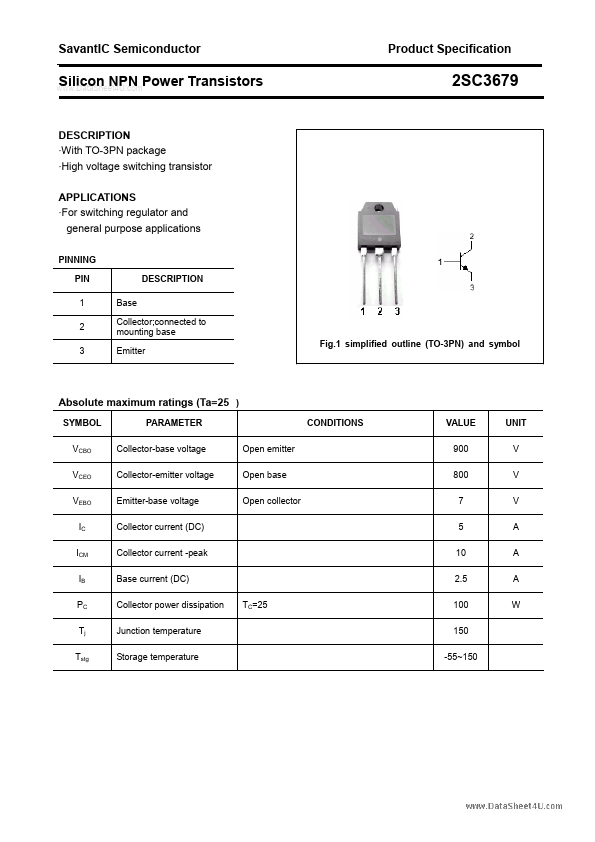
PINNING PIN 1 2 3 Base Collector;connected to mounting base Emitter Fig.1 simplified outline (TO-3PN) and symbol...