Datasheet Summary
SavantIC Semiconductor
..
Product Specification
Silicon NPN Power Transistors
DESCRIPTION
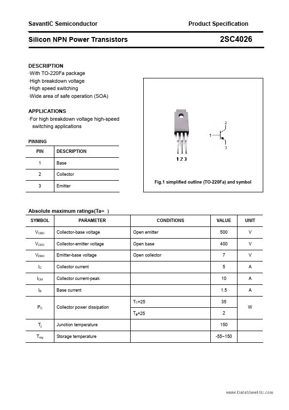
- With TO-220Fa package
- High breakdown voltage
- High speed switching
- Wide area of safe operation (SOA) APPLICATIONS
- For high breakdown voltage high-speed switching applications
PINNING PIN 1 2 3 DESCRIPTION Base Collector Emitter Fig.1 simplified outline (TO-220Fa) and...