With TO-3 package High breakdown voltage
APPLICATIONS For use in audio and general purpose applications
PINNING (See Fig.2) PIN DESCRIPTION
1 Base
2 Emitter
3 Collector
Fig.1 simplified outline (TO-3) and symbol
Absolute maximum ratings(Ta=25 )
SYMBOL
PARAMETER
VCBO
Collector-base voltage
VCE
The following content is an automatically extracted verbatim text
from the original manufacturer datasheet and is provided for reference purposes only.
View original datasheet text
Product Specification
Silicon NPN Power Transistors
www.jmnic.com
2SC1050
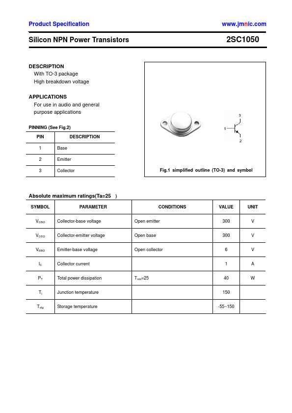
DESCRIPTION With TO-3 package High breakdown voltage
APPLICATIONS For use in audio and general purpose applications
PINNING (See Fig.2) PIN DESCRIPTION
1 Base
2 Emitter
3 Collector
Fig.