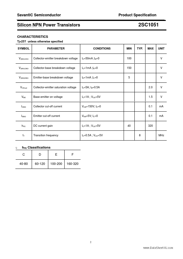
Datasheet Summary
SavantIC Semiconductor
Swwiwli.DcaotanSheNet4PU.NPower Transistors
DESCRIPTION
- With TO-3 package
- Wide area of safe operation
APPLICATIONS
- For low frequency power amplifier and large power switching applications
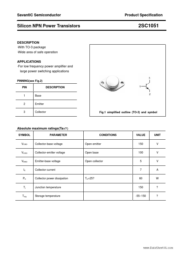
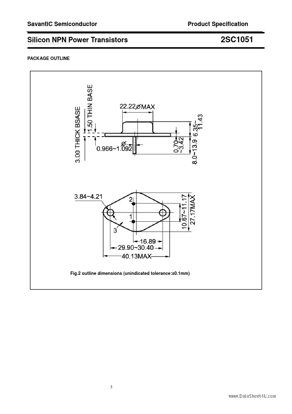
PINNING(see Fig.2) PIN DESCRIPTION 1 Base 2 Emitter 3 Collector
Product Specification
2SC1051
Fig.1 simplified outline (TO-3) and...