C4662 Overview
Key Specifications
Height: 42.85 mm
Length: 50.8 mm
Max Operating Temp: 85 °C
Min Operating Temp: -40 °C
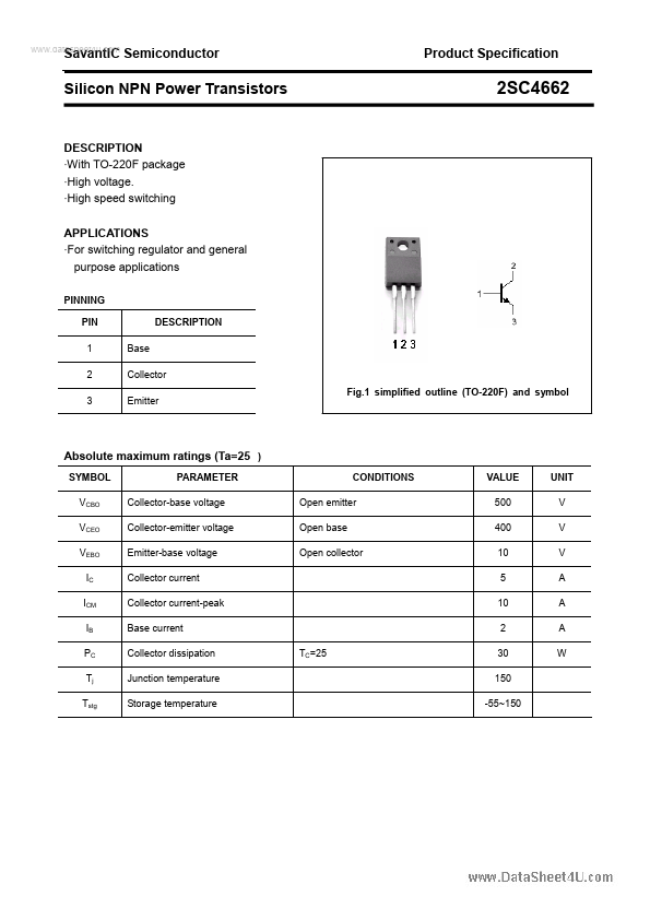
Description
With TO-220F package - High voltage. High speed switching.
| Part | C4662 |
|---|---|
| Description | 2SC4662 |
| Manufacturer | SavantIC |
| Size | 265.98 KB |
Height: 42.85 mm
Length: 50.8 mm
Max Operating Temp: 85 °C
Min Operating Temp: -40 °C
With TO-220F package - High voltage. High speed switching.
| Seller | Inventory | Price Breaks | Buy |
|---|---|---|---|
| DigiKey | 0 | 3+ : 119.61333 USD | View Offer |
| Sager Electronics | 0 | 1+ : 182.68 USD 15+ : 123.5 USD 43+ : 78.29 USD 130+ : 62.19 USD |
View Offer |
| Part Number | Manufacturer | Description |
|---|---|---|
| C4666 | Toshiba | 2SC4666 |
| C4660 | SANYO | 2SC4660 |
| C4664 | Shindengen | 2SC4664 |
| C4667 | Toshiba | 2SC4667 |