www.dat
aWshiethet4TuO.co-
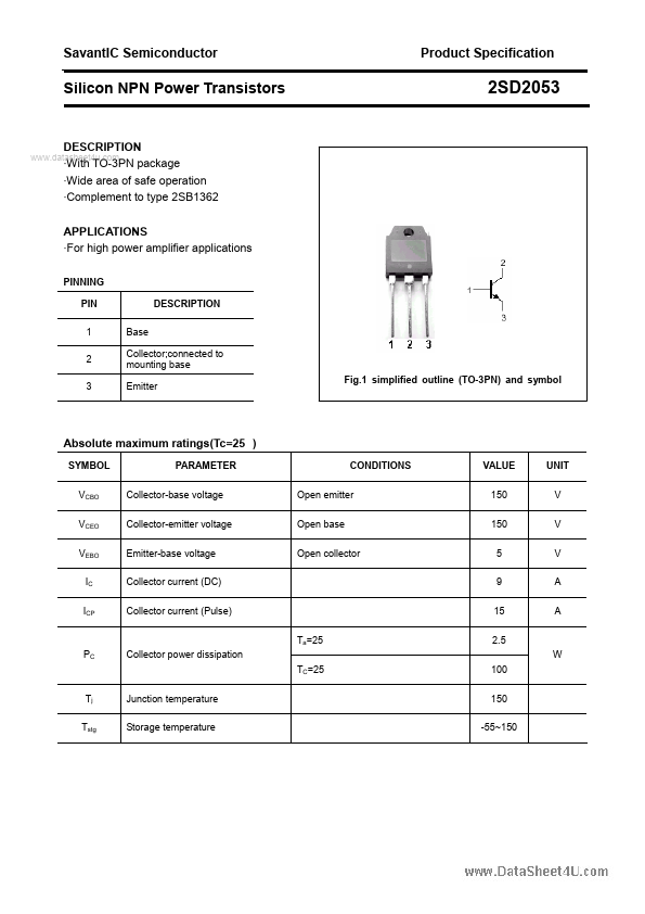
3mPN package
Wide area of safe operation
Complement to type 2SB1362
APPLICATIONS
For high power amplifier applications
PINNING PIN 1 2 3
DESCRIPTION
Base Collector;connected to mounting base Emitter
Fig.1 simplified outline (TO-3PN) and symbol
Absolu
The following content is an automatically extracted verbatim text
from the original manufacturer datasheet and is provided for reference purposes only.
View original datasheet text
SavantIC Semiconductor
Silicon NPN Power Transistors
Product Specification
2SD2053
DESCRIPTION www.dat·aWshiethet4TuO.co-3mPN package
·Wide area of safe operation
·Complement to type 2SB1362
APPLICATIONS ·For high power amplifier applications
PINNING PIN 1 2 3
DESCRIPTION
Base Collector;connected to mounting base Emitter
Fig.1 simplified outline (TO-3PN) and symbol
Absolute maximum ratings(Tc=25 )
SYMBOL
PARAMETER
VCBO
Collector-base voltage
VCEO VEBO
IC ICP
Collector-emitter voltage Emitter-base voltage Collector current (DC) Collector current (Pulse)
PC Collector power dissipation
Tj Junction temperature Tstg Storage temperature
CONDITIONS Open emitter Open base Open collector
Ta=25 TC=25
VALUE 150 150 5 9 15 2.