SeCoS Halbleitertechnologie GmbH 2SC3930
NPN Silicon Transistor
| Part No. | 2SC3930 |
|---|---|
| Datasheet | 2SC3930 Download |
| Manufacturer |  SeCoS Halbleitertechnologie GmbH |
| Description | NPN Silicon Transistor |
| Buy | Stock & Price |

ABSOLUTE MAXIMUM RATINGS
( TA = 25°C unless otherwise specified) Parameter Collector to Base Voltage Collector to Emitter Voltage Emitter to Base Voltage Collector Current – Continuous Collector Power Dissipation Junction, Storage Temperature Symbol VCBO VCEO VEBO IC PC TJ, TSTG Ratings 30 20 5 30 150 150, -55~150 Unit V V V mA mW ℃ELECTRICAL CHARACTERISTICS
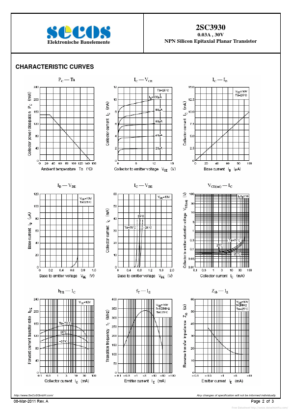
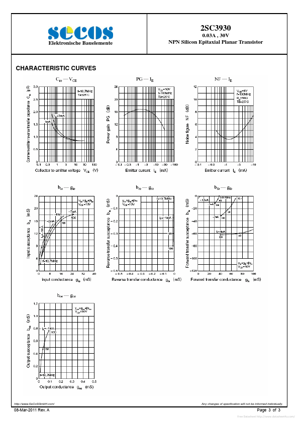
( TA = 25°C unless otherwise specified) Parameter Collector-base breakdown voltage Collector-emitter breakdown voltage Emitter-base breakdown voltage Collector Cut-off Current Emitter Cut-off Current DC Current Gain Transition Frequency Common emitter capacitance Noise Figure Reverse transfer impedance Symbol V(BR)CBO V(BR)CEO V(BR)EBO ICBO IEBO hFE fT Min. 30 20 5 70 150 - Typ. - Max. 0.1 0.1 220 1.5 4 50 Unit V V V A A MHz pF dB Ω Testing Condition IC=100μA, IE=0 IC=100μA, IB=0 IE=100μA, IC=0 VCB=10V, IE=0 VEB=5V, IC=0 VCE=10V, IC=1mA VCE=10V, IE=1mA, f=200MHz VCB=10V, IC=1mA, f=10.7MHz VCB=10V, IC=1mA, f=5MHz VCB=10V, IC=1mA, f=2MHz reverse transfer Cre NF Zrb Any changes of specification will not be informed individually.