SeCoS Halbleitertechnologie GmbH A1015
PNP Transistor
| Part No. | A1015 |
|---|---|
| Datasheet | A1015 Download |
| Manufacturer |  SeCoS Halbleitertechnologie GmbH |
| Description | PNP Transistor |
| Buy | Stock & Price |
FEATURES
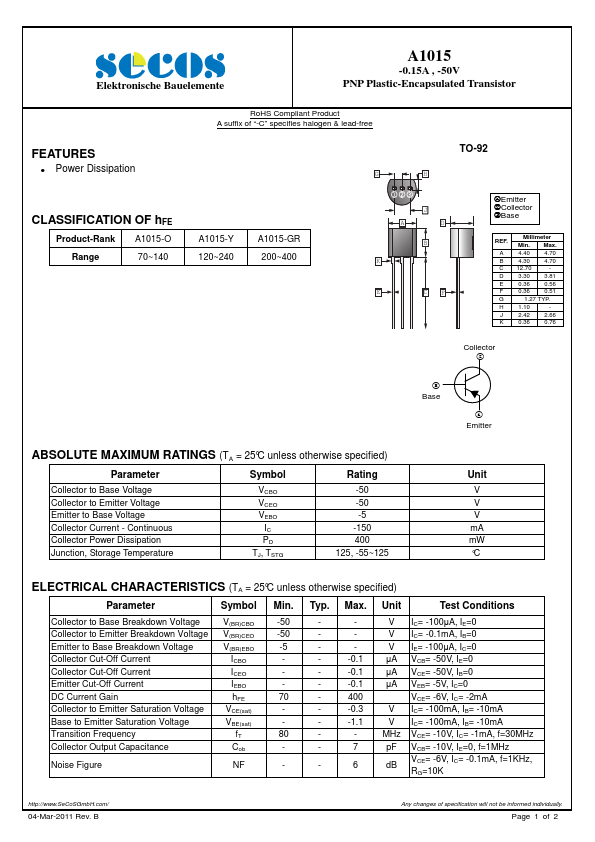
Power Dissipation CLASSIFICATION OF hFE Product-Rank A1015-O Range 70~140 RoHS Compliant Product A suffix of “-C” specifies halogen & lead-free TO-92 GH A1015-Y 120~240 A1015-GR 200~400 J AD B K E CF 1Emitter 2Collector 3Base REF. A B C D E F G H J K Millimeter Min. Max. 4.40 4.70 4.30 4.70 12.70 - 3.30 3.81 0.36 0.56 0.36 0.51 1.27 TYP. 1.10 - 2.42 2.66 0.36 0.76 Collector 2 3 Base 1 EmitterABSOLUTE MAXIMUM RATINGS
(TA = 25°C unless otherwise specified) Parameter Symbol Rating Collector to Base Voltage Collector to Emitter Voltage Emitter to Base Voltage Collector Current - Continuous Collector Power Dissipation Junction, Storage Temperature VCBO VCEO VEBO IC PD TJ, TSTG -50 -50 -5 -150 400 125, -55~125 Unit V V V mA mW °CELECTRICAL CHARACTERISTICS
(TA = 25°C unless otherwise specified) Parameter Symbol Min. Typ. Max. Unit Test Conditions Collector to Base Breakdown Voltage V(BR)CBO -50 - - V IC= -100µA, IE=0 Collector to Emitter Breakdown Voltage V(BR)CEO -50 - - V IC= -0.