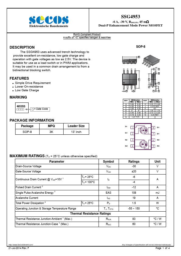
Download SSG4953 Datasheet PDF
SSG4953 page 2
Page 2
SSG4953 page 3
Page 3

SSG4953 Description

The SSG4953 uses advanced trench technology to provide excellent on-resistance, low gate charge and operation with gate voltages as low as 2.5V. The device is suitable for use as a load switch or in PWM applications. It may be used in a mon drain arrangement to from a bidirectional blocking switch.

SSG4953 Key Features

  • Simple Drive Requirement
  • Lower On-resistance
  • Low Gate Charge
  • 30 ±20 -6 -4 -12 108 19 1.5 -55 ~ 150
  • 6 A, -30 V, RDS(ON) 45 m Dual-P Enhancement Mode Power MOSFET
  • S VDS= -10V, ID= -6A
  • 1 μA VDS= -24V,VGS=0
  • 3.1 -9
  • ID= -6A nC VDS= -20V
  • VGS=0V