Datasheet4U Logo Datasheet4U.com

SST2623 - P-Channel MOSFET

General Description

0.37Ref.

0.20 0.60 Ref.

The SST2623 utiltzed advance processing techniques to achieve the lowest possible on-resistance, extermely efficient and cost-effectiveness device.

Key Features

  • Low On-Resistance.
  • Low Gate Charge D1 D2 Dimensions in millimeters D1 6 S1 5 D2 4 G1 G2 Date Code 2623 S1 S2 1 G1 2 S2 3 G2 Absolute Maximum Ratings Parameter Drain-Source Voltage Gate-Source Voltage Continuous Drain Current 3 Continuous Drain Current 3 Pulsed Drain Current 1 Total Power Dissipation Linear Derating Factor Operating Junction and Storage Temperature Range Tj, Tstg Symbol VDS VGS ID@TA=25 C ID@TA=70 C IDM PD@TA=25 C o o o Ratings -30 ±20 -2 -1.6 -20 1.2 0.

📥 Download Datasheet

Full PDF Text Transcription (Reference)

The following content is an automatically extracted verbatim text from the original manufacturer datasheet and is provided for reference purposes only.

View original datasheet text
www.DataSheet4U.com SST2623 -2A, -30V,RDS(ON) 170m£[ Elektronische Bauelemente P-Channel Enhancement Mode Power Mos.FET RoHS Compliant Product SOT-26 Description 0.37Ref. 0.20 0.60 Ref. 
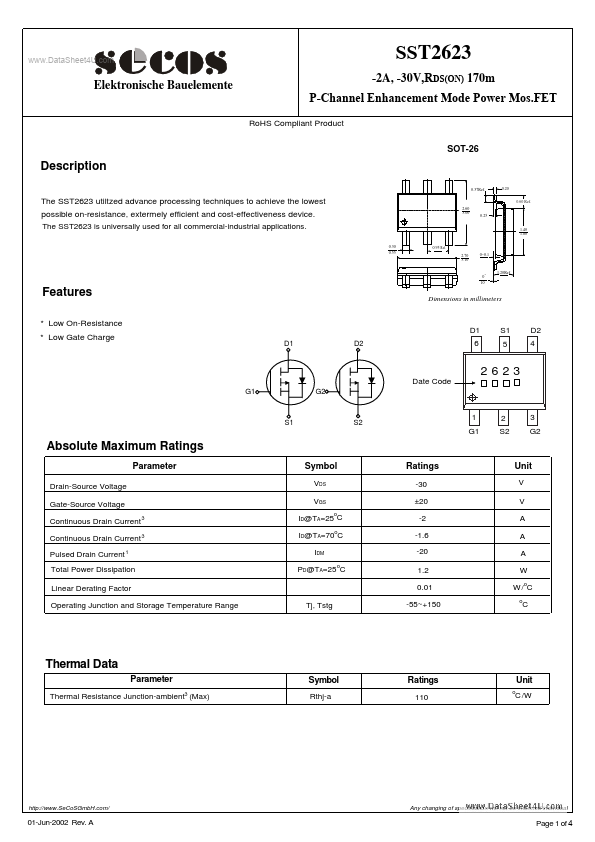
2.60 3.00 The SST2623 utiltzed advance processing techniques to achieve the lowest possible on-resistance, extermely efficient and cost-effectiveness device. The SST2623 is universally used for all commercial-industrial applications. 0.30 0.55 0.95 Ref. 2.70 3.10 0~0.1 0.25 1.40 1.80 0 o 10 o 1.20Ref.