IRF460
IRF460 is N-Channel Power MOSFET manufactured by Seme LAB.
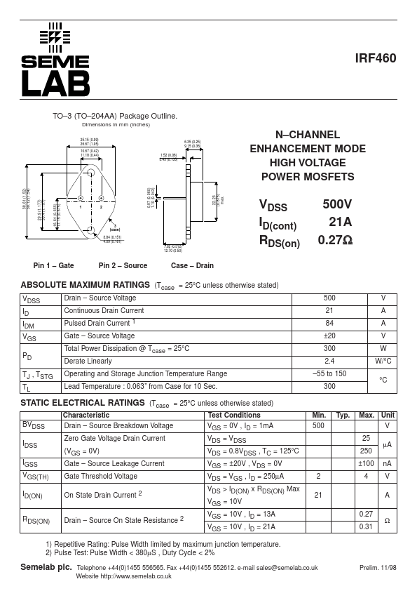
TO- 3 (TO- 204AA) Package Outline.
Dimensions in mm (inches)
25.15 (0.99) 26.67 (1.05) 10.67 (0.42) 11.18 (0.44) 1.52 (0.06) 3.43 (0.135) 6.35 (0.25) 9.15 (0.36)
N- CHANNEL ENHANCEMENT MODE HIGH VOLTAGE POWER MOSFETS
22.23 (0.875) max.
38.61 (1.52) 39.12 (1.54)
0.97 (0.060) 1.10 (0.043)
3 (case) 3.84 (0.151) 4.09 (0.161) 7.92 (0.312) 12.70 (0.50)
VDSS ID(cont) RDS(on)
500V 21A 0.27Ω
29.9 (1.177) 30.4 (1.197)
Pin 1
- Gate
16.64 (0.655) 17.15 (0.675)
Pin 2
- Source
Case
- Drain
ABSOLUTE MAXIMUM RATINGS (Tcase = 25°C unless otherwise stated)
VDSS ID IDM VGS PD TJ , TSTG TL Drain
- Source Voltage Continuous Drain Current Pulsed Drain Current 1 Gate
- Source Voltage Total Power Dissipation @ Tcase = 25°C Derate Linearly Operating and Storage Junction Temperature Range Lead Temperature : 0.063” from Case for 10 Sec. 500 21 84 ±20 300 2.4
- 55 to 150 300 V A A V W W/°C °C
STATIC ELECTRICAL RATINGS (Tcase = 25°C unless otherwise stated)
BVDSS IDSS IGSS VGS(TH) ID(ON) RDS(ON) Characteristic Drain
- Source Breakdown Voltage Zero Gate Voltage Drain Current (VGS = 0V) Gate
- Source Leakage Current Gate Threshold Voltage On State Drain Current 2 Drain
- Source On State Resistance 2 Test Conditions VGS = 0V , ID = 1m A VDS = VDSS VDS = 0.8VDSS , TC = 125°C VGS = ±20V , VDS = 0V VDS = VGS , ID = 250µA VDS > ID(ON) x RDS(ON) Max VGS = 10V VGS = 10V , ID = 13A VGS = 10V , ID = 21A 2 21 0.27 0.31 Min. 500 Typ. Max. Unit V 25 250 ±100 4 µA n A V A Ω
1) Repetitive Rating: Pulse Width limited by maximum junction temperature. 2) Pulse Test: Pulse Width < 380µS , Duty Cycle < 2%
Semelab plc.
Telephone +44(0)1455 556565. Fax +44(0)1455 552612. e-mail sales@semelab.co.uk Website http://.semelab.co.uk
Prelim. 11/98
DYNAMIC CHARACTERISTICS
Characteristic Ciss Coss Crss Qg Qgs Qgd td(on) tr td(off) tf Input Capacitance Output Capacitance Reverse Transfer Capacitance Total Gate Charge3 Gate
- Source Charge Gate
- Drain (“Miller”) Charge Turn- on Delay Time Rise...