IRFY140C
IRFY140C is N-CHANNEL POWER MOSFET manufactured by Seme LAB.
FEATURES
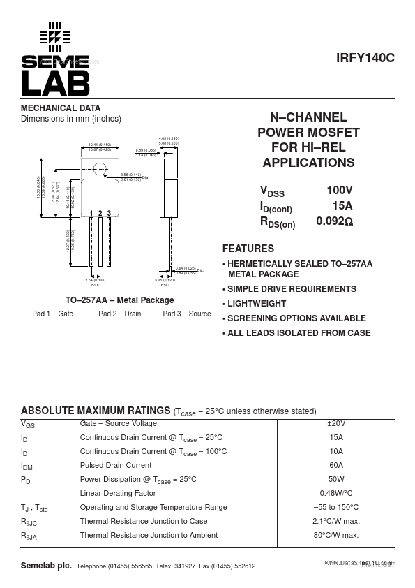
16.38 (0.645) 16.89 (0.665)
13.38 (0.527) 13.64 (0.537)
3.56 (0.140) Dia. 3.81 (0.150)
1 2 3
12.07 (0.500) 19.05 (0.750)
100V 15A 0.092Ω
10.41 (0.410) 10.92 (0.430)
0.64 (0.025) Dia. 0.89 (0.035) 2.54 (0.100) BSC 3.05 (0.120) BSC
- HERMETICALLY SEALED TO- 257AA METAL PACKAGE
- SIMPLE DRIVE REQUIREMENTS
- LIGHTWEIGHT
- SCREENING OPTIONS AVAILABLE
- ALL LEADS ISOLATED FROM CASE
TO- 257AA
- Metal Package
Pad 1
- Gate Pad 2
- Drain Pad 3
- Source
ABSOLUTE MAXIMUM RATINGS (Tcase = 25°C unless otherwise stated)
VGS ID ID IDM PD TJ , Tstg RθJC RθJA Gate
- Source Voltage Continuous Drain Current @ Tcase = 25°C Continuous Drain Current @ Tcase = 100°C Pulsed Drain Current Power Dissipation @ Tcase = 25°C Linear Derating Factor Operating and Storage Temperature Range Thermal Resistance Junction to Case Thermal Resistance Junction to Ambient ±20V 15A 10A 60A 50W 0.48W/°C
- 55 to 150°C 2.1°C/W max. 80°C/W max.
Semelab plc.
Telephone (01455) 556565. Telex: 341927. Fax (01455) 552612.
Prelim. 6/97
..
ELECTRICAL CHARACTERISTICS (TC = 25°C unless otherwise stated)
Parameter
BVDSS ∆TJ RDS(on) STATIC ELECTRICAL RATINGS Drain
- Source Breakdown Voltage Breakdown Voltage Static Drain
- Source On- State Resistance Forward Transconductance Zero Gate Voltage Drain Current Forward Gate
- Source Leakage Reverse Gate
- Source Leakage DYNAMIC CHARACTERISTICS Input Capacitance Output Capacitance Reverse Transfer Capacitance Total Gate Charge Gate
- Source Charge Gate
- Drain (“Miller”) Charge Turn- On Delay Time Rise Time Turn- Off Delay Time Fall Time
Test Conditions
VGS = 0 ID = 1m A VGS = 10V VDS = VGS VDS ≥ 15V VGS = 0 VGS = 20V VGS =
- 20V VGS = 0 VDS = 25V f = 1MHz VGS = 10V VDS = 0.5BVDSS ID = 15A VDS = 0.5BVDSS VDD = 50V ID = 15A RG = 9.1Ω ID = 15A ID = 12A ID = 250µA IDS = 12A VDS = 0.8BVDSS TJ = 125°C ID = 1m...