SM840S
Features
- Low Intrinsic Capacitances
- Excellent Switching Characteristics
- Extended Safe Operating Area
- Unrivalled Gate Charge : 28 n C (Typ.)
- BVDSS=500V,ID=9A
- Lower RDS(on) : 0.75 Ω (Max) @VG=10V
- 100% Avalanche Tested
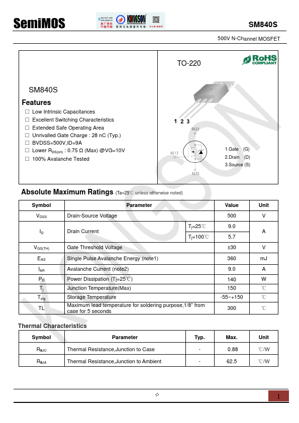
1.Gate (G) 2.Drain (D) 3.Source (S)
Absolute Maximum Ratings (Ta=25℃ unless otherwise noted)
Symbol VDSS
VGS(TH) EAS IAR PD Tj Tstg TL
Parameter
Drain-Source Voltage Drain Current Gate Threshold Voltage
Tj=25℃ Tj=100℃
Single Pulse Avalanche Energy (note1)
Avalanche Current (note2) Power Dissipation (Tj=25℃)
Junction Temperature(Max)
Storage Temperature Maximum lead temperature for soldering purpose,1/8” from case for 5 seconds
Value 500 9.0 5.7 ±30 360 9.0 140 150 -55~+150 300
Unit V
V m J A W ℃ ℃ ℃
Thermal Characteristics
Symbol
Parameter
Typ.
Max.
Unit
RθJC
Thermal Resistance,Junction to Case
- 0.88
℃/W
RθJA
Thermal Resistance,Junction to Ambient
- 62.5
℃/W
Electrical Characteristics (Ta=25℃ unless otherwise...