SRDA3.3-6 Overview
Key Specifications
Package: SOIC
Mount Type: Surface Mount
Pins: 8
Operating Voltage: 3.3 V
Description
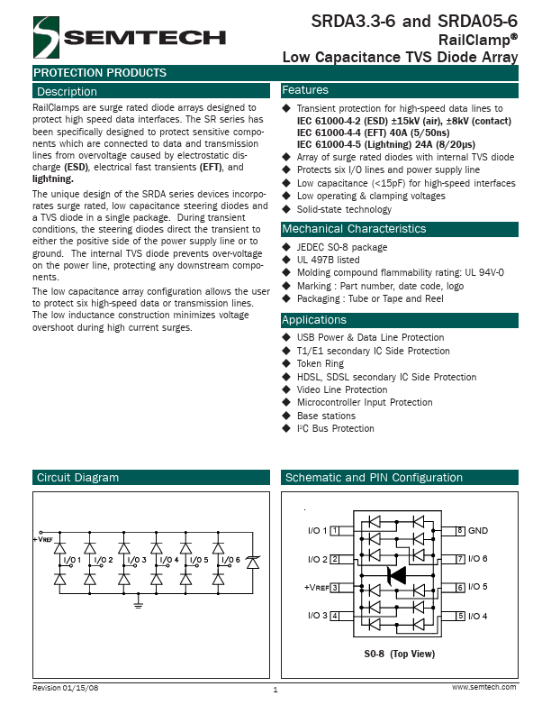
RailClamps are surge rated diode arrays designed to protect high speed data interfaces. The SR series has been specifically designed to protect sensitive components which are connected to data and transmission lines from overvoltage caused by electrostatic discharge (ESD), electrical fast transients (EFT), and lightning.