LH28F400SU-LC
Overview
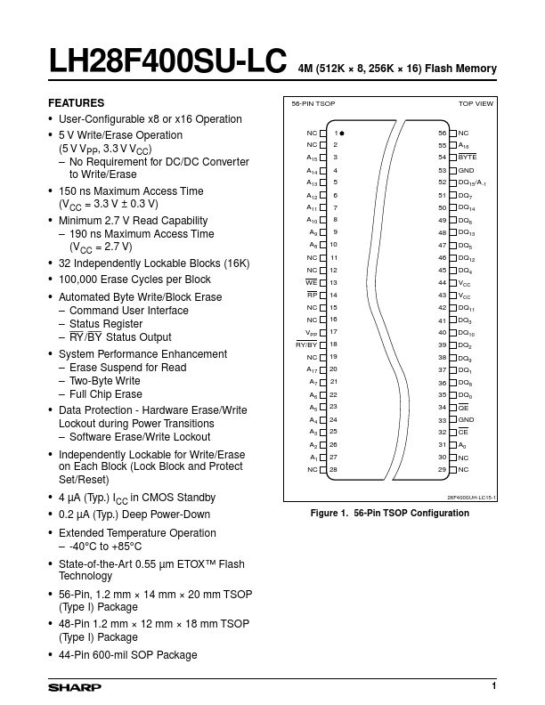
- User-Configurable x8 or x16 Operation 4M (512K × 8, 256K × 16) Flash Memory
| Part | LH28F400SU-LC |
|---|---|
| Description | 4M (512K bb 8/ 256K bb 16) Flash Memory |
| Manufacturer | Sharp Corporation |
| Size | 299.38 KB |
| Part Number | Manufacturer | Description |
|---|---|---|
| W25Q256JV | Winbond | 3V 256M-BIT SERIAL FLASH MEMORY |
| W25Q128JV | Winbond | 3V 128M-BIT SERIAL FLASH MEMORY |
| 25Q128JVSM | Winbond | 3V 128M-BIT SERIAL FLASH MEMORY |