Datasheet4U Logo Datasheet4U.com

LH28F400SUB-Z0 - 4M (512K bb 8/ 256K bb 16) Flash Memory

Datasheet Summary

Description

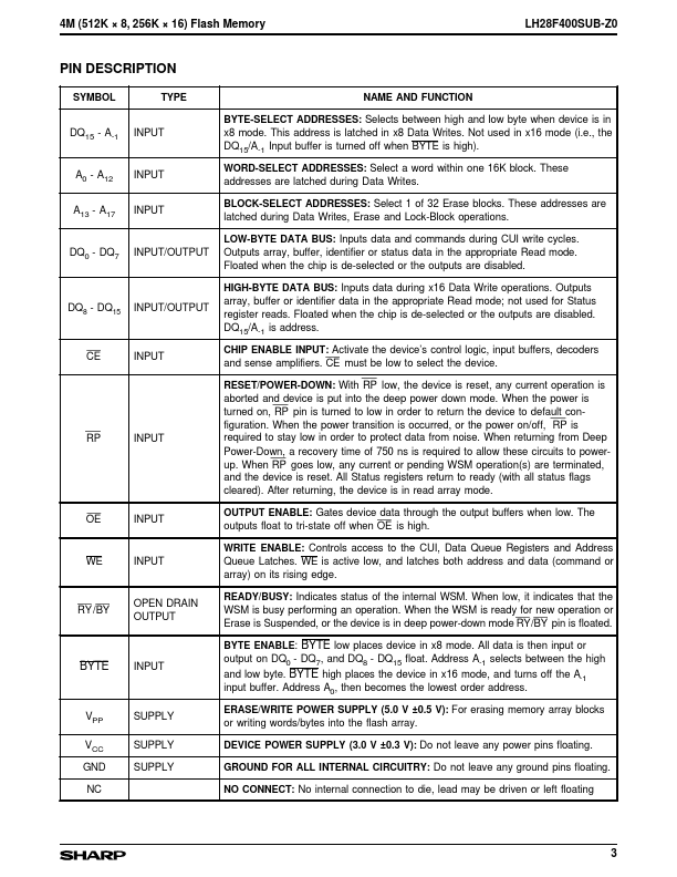
SYMBOL TYPE NAME AND FUNCTION BYTE-SELECT ADDRESSES: Selects between high and low byte when device is in x8 mode.

This address is latched in x8 Data Writes.

Not used in x16 mode (i.e., the DQ15/A-1 Input buffer is turned off when BYTE is high).

Features

  • 49-PIN CSP 4M (512K × 8, 256K × 16) Flash Memory TOP VIEW.
  • User-Configurable x8 or x16 Operation.
  • 5 V Write/Erase Operation (5 V VPP, 3.3 V VCC).
  • No Requirement for DC/DC Converter to Write/Erase 1 A B C D E A1 A2 A3 A0 OE 2 A4 A5 A6 DQ9 DQ1 DQ8 DQ0 3 A7 A17 RY/BY NC DQ3 DQ10 DQ2 4 VPP RP NC NC DQ11 VCC VCC 5 A9 A8 WE NC DQ4 6 A12 A11 A10 DQ13 DQ6 7 A15 A14 A13 A16 DQ15/ A -1.
  • 150 ns Maximum Access Time (VCC = 3.3 V ± 0.3 V).
  • Min. 2.7 V Rea.

📥 Download Datasheet

Datasheet preview – LH28F400SUB-Z0

Datasheet Details

Part number LH28F400SUB-Z0
Manufacturer Sharp Electrionic Components
File Size 277.07 KB
Description 4M (512K bb 8/ 256K bb 16) Flash Memory
Datasheet download datasheet LH28F400SUB-Z0 Datasheet
Additional preview pages of the LH28F400SUB-Z0 datasheet.
Other Datasheets by Sharp Electrionic Components

Full PDF Text Transcription

Click to expand full text
LH28F400SUB-Z0 FEATURES 49-PIN CSP 4M (512K × 8, 256K × 16) Flash Memory TOP VIEW • User-Configurable x8 or x16 Operation • 5 V Write/Erase Operation (5 V VPP, 3.3 V VCC) – No Requirement for DC/DC Converter to Write/Erase 1 A B C D E A1 A2 A3 A0 OE 2 A4 A5 A6 DQ9 DQ1 DQ8 DQ0 3 A7 A17 RY/BY NC DQ3 DQ10 DQ2 4 VPP RP NC NC DQ11 VCC VCC 5 A9 A8 WE NC DQ4 6 A12 A11 A10 DQ13 DQ6 7 A15 A14 A13 A16 DQ15/ A -1 • 150 ns Maximum Access Time (VCC = 3.3 V ± 0.3 V) • Min. 2.7 V Read Capability – 160 ns Maximum Access Time (VCC = 2.7 V) F GND G CE DQ12 DQ14 GND DQ5 DQ7 BYTE • 32 Independently Lockable Blocks (16K) • 100,000 Erase Cycles per Block • Automated Byte Write/Block Erase – Command User Interface – Status Register – RY  / » BY  » Status Output 28F400SUB-1 Figure 1.
Published: |