Sharp LH28F008SA
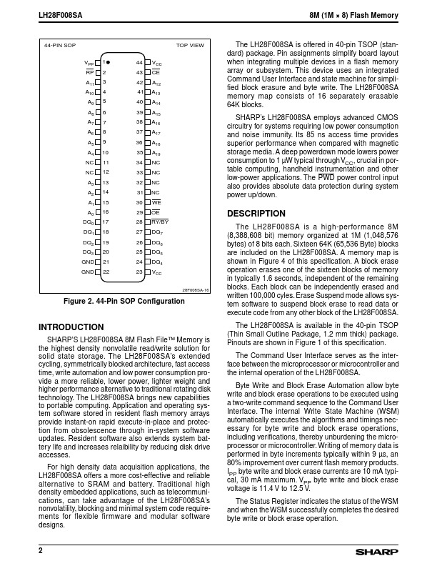
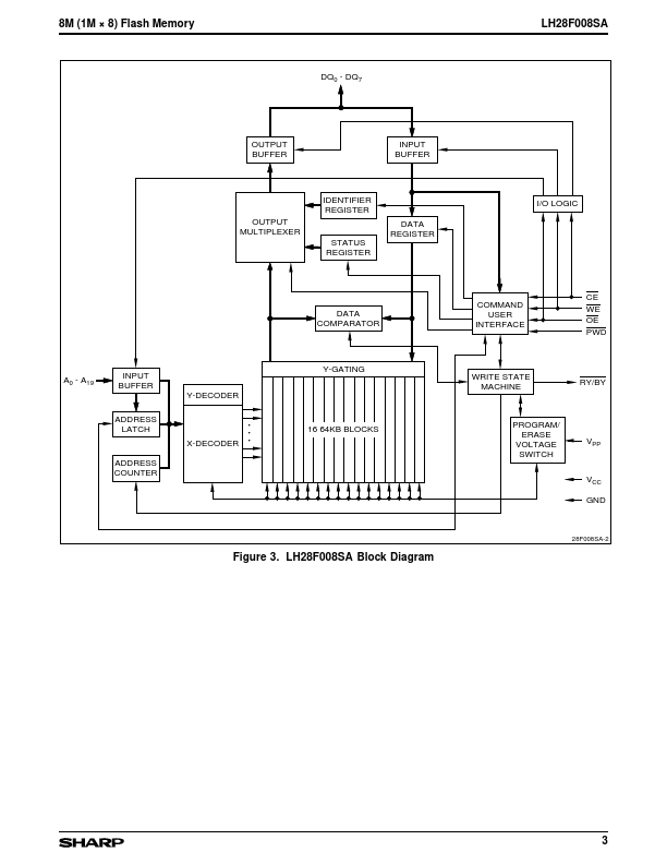
The LH28F008SA is offered in 40-pin TSOP (standard) package. This device uses an integrated Command User Interface and state machine for simplified block erasure and byte write. The LH28F008SA memory map consists of 16 separately erasable 64K blocks.| Part No. | LH28F008SA |
|---|---|
| Datasheet | LH28F008SA Download |
| Manufacturer |  Sharp |
| Description | 8M (1M x 8) Flash Memory |
| Buy | Stock & Price |
FEATURES
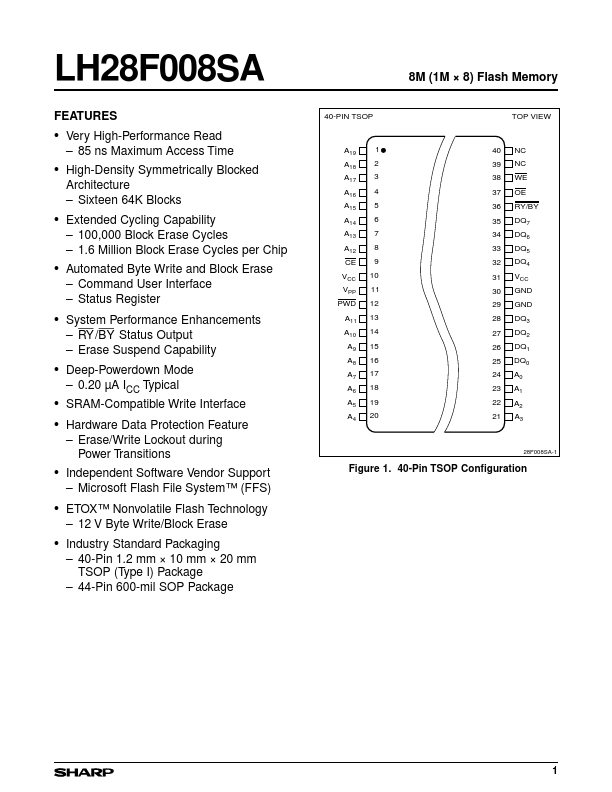
40-PIN TSOP 8M (1M × 8) Flash Memory TOP VIEW● Very High-Performance Read – 85 ns Maximum Access Time A19 A18 A17 A16 A15 A14 A13 A12 CE VCC VPP PWD A11 A10 A9 A8 A7 A6 A5 A4 1 2 3 4 5 6 7 8 9 10 11 12 13 14 15 16 17 18 19 20 40 39 38 37 36 35 34 33 32 31 30 29 28 27 26 25 24 23 22 21 NC NC WE OE RY/BY DQ7 DQ6 DQ5 DQ4 VCC GND GND DQ3 DQ2 DQ1 DQ0 A0 A1 A2 A3
● High-Density Symmetrically Blocked Architecture – Sixteen 64K Blocks
● Extended Cycling Capability – 100,000 Block Erase Cycles – 1.6 Million Block Erase Cycles per Chip
● Automated Byte Write and Block Erase – Command User Interface – Status Register
● System Performance Enhancements – RY / » BY » Status Output – Erase Suspend Capability
● Deep-Powerdown Mode – 0.20 µA ICC Typical
● SRAM-Compatible Write Interface
● Hardware Data Protection Feature – Erase/Write Lockout during Power Transitions 28F008SA-1
● Independent Software Vendor Support – Microsoft Flash File System™ (FFS) Figure 1. 40-Pin TSOP Configuration
● ETO...