PC66-222-620
PC66-222-620 is 3.3V 4M x 64/72-Bit 1 BANK SDRAM Module 3.3V 8M x 64/72-Bit 2 BANK SDRAM Module manufactured by Siemens Semiconductor Group.
3.3V 4M x 64/72-Bit 1 BANK SDRAM Module 3.3V 8M x 64/72-Bit 2 BANK SDRAM Module
HYS64(72)V4200GU HYS64(72)V8220GU
PC66 & PC100 168 pin unbuffered DIMM Modules
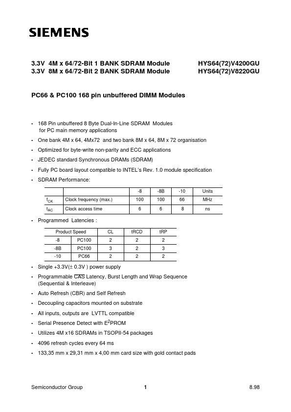
- 168 Pin unbuffered 8 Byte Dual-In-Line SDRAM Modules for PC main memory applications One bank 4M x 64, 4Mx72 and two bank 8M x 64, 8M x 72 organisation Optimized for byte-write non-parity and ECC applications JEDEC standard Synchronous DRAMs (SDRAM) Fully PC board layout patible to INTEL’s Rev. 1.0 module specification SDRAM Performance:
-8 f CK t AC Clock frequency (max.) Clock access time 100 6 -8B 100 6 -10 66 8 Units MHz ns
- -
- -
- -
Programmed Latencies :
Product Speed -8 -8B -10 PC100 PC100 PC66 CL 2 3 2 t RCD 2 2 2 t RP 2 3 2
- -
Single +3.3V(± 0.3V ) power supply Programmable CAS Latency, Burst Length and Wrap Sequence (Sequential & Interleave) Auto Refresh (CBR) and Self Refresh Decoupling capacitors mounted on substrate All inputs, outputs are LVTTL patible Serial Presence Detect with E2PROM Utilizes 4M x16 SDRAMs in TSOPII-54 packages 4096 refresh cycles every 64 ms 133,35 mm x 29,31 mm x 4,00 mm card size with gold contact pads
- -
- -
- -
- Semiconductor Group
HYS64(72)V4200/8220GU SDRAM-Modules
The HYS64(72)V4200 and HYB64(72)V8220 are an industry standard 168-pin 8-byte Dual in-line Memory Module (DIMM) which are organised as 4M x 64, 4M x 72 in an one bank and 8M x 64, 8M x72 in two banks high speed memory arrays designed with 64Mbit Synchronous DRAMs (SDRAMs Die Rev.B) for non-parity and ECC application. The DIMMs use -8 and -8B speed sort 4M x 16 SDRAM devices in TSOP54 packages to meet the PC100 requirements and -10 parts for 66 MHz bus speed applications. Decoupling capacitors are mounted on the PC board. The PC board design is according to INTEL’s module specification. The DIMMs have a serial presence detect, implemented with a serial E2PROM using the two pin I2C protocol. The first 128 bytes are utilized by the DIMM manufacturer and the second 128 bytes are...