SIS5501
SIS5501 is PCI/ISA Cache Memory Controller manufactured by Silicon Integrated System.
- Part of the SIS5502 comparator family.
- Part of the SIS5502 comparator family.
.. Pentium/P54C PCI/ISA Chipset
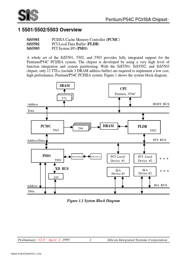
1 5501/5502/5503 Overview
SiS5501 SiS5502 SiS5503 PCI/ISA Cache Memory Controller (PCMC) PCI Local Data Buffer (PLDB) PCI System I/O (PSIO)
A whole set of the SiS5501, 5502, and 5503 provides fully integrated support for the Pentium/P54C PCI/ISA system. The chipset is developed by using a very high level of function integration and system partitioning. With the SiS5501, SiS5502, and SiS5503 chipset, only 12 TTLs (include 3 DRAM address buffer) are required to implement a low cost, high performance, Pentium/P54C PCI/ISA system. Figure 1 shows the system block diagram.
SRAM
Pentium , P54C
373 Address Data HOST BUS
PCMC
5501...