SiS5596
SiS5596 is PCI Memory & VGA Controller manufactured by Silicon Integrated System.
Overview
Si S5596
PCI, Memory & VGA Controller
Si S5513
PCI System I/O
The Si S5596/5513 with built-in VGA controller is a two-chip solution for Pentium PCI/ISA system. A portion of on board DRAM is shared with the built-in VGA controller. In that way, the system cost is substantially reduced.
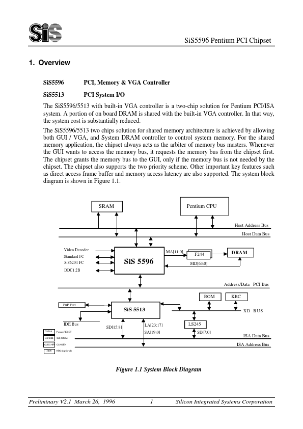
The Si S5596/5513 two chips solution for shared memory architecture is achieved by allowing both GUI / VGA, and System DRAM controller to control system memory. For the shared memory application, the chipset always acts as the arbiter of memory bus masters. Whenever the GUI wants to access the memory bus, it requests the memory bus from the chipset first. The chipset grants the memory bus to the GUI, only if the memory bus is not needed by the chipset. The chipset also supports the two priority scheme. Other important key features such as direct access frame buffer and memory access latency are also supported. The system block diagram is shown in Figure 1.1.
SRAM
Pentium CPU
Video Decoder Standard FC Si S6204 FC DDC1,2B
Pn P Port
IDE Bus
74F04 Power,RESET 74F244 SA,14Mhz CLKCHIP CLKGEN 7406 KBC (optional)
Si S 5596
MA[11:0]
F244
MD[63:0]
Host Address Bus Host Data Bus
DRAM
Si S 5513
SD[15:8]
LA[23:17] SA[19:0]
Address/Data PCI Bus
LS245
SD[7:0]
XD BUS
ISA Data Bus ISA Address Bus
Figure 1.1 System Block Diagram
Preliminary V2.1 March 26, 1996
Silicon Integrated Systems Corporation
Si S5596 Pentium PCI Chipset
1.1 General Features
- Supports Intel Pentium CPU and other patible CPU at 66/60/50MHz (external clock speed)
- Supports VGA Shared Memory Architecture
- Direct Memory Accesses
- Shared Memory Area 0.5M, 1M, 1.5M, 2M, 2.5M, 3M, 3.5M, 4M.
- Built-in 2-Priority...